Reworking device for optical COB package

An optical and heating component technology, applied in the field of optical communication, can solve problems such as damage to PD, failure to meet standards, and device scrapping

Pending Publication Date: 2019-03-26
LINKTEL TECH CO LTD
View PDF21 Cites 2 Cited by
  • Summary
  • Abstract
  • Description
  • Claims
  • Application Information

AI Technical Summary

Problems solved by technology

[0004] During the production process, the coupling operation may damage the PD, or poor incoming materials may cause the coupled module to fail to work or the parameters are not up to standard. At this time, the module needs to be repaired.
At present, the rework measures taken for COB packaged devices in the production process are basically based on pure manual operation, or the problem of rework yield is basically not reworked, and they are directly scrapped; because the patch on the PCBA will be damaged when the rework is removed. The PCBA is also damaged, and finally the device is scrapped, and the repair yield is not high.

Method used


Image

  • Reworking device for optical COB package
  • Reworking device for optical COB package
  • Reworking device for optical COB package

Examples


Embodiment Construction

[0032] The following will clearly and completely describe the technical solutions in the embodiments of the present invention with reference to the accompanying drawings in the embodiments of the present invention. Obviously, the described embodiments are only some, not all, embodiments of the present invention. Based on the embodiments of the present invention, all other embodiments obtained by persons of ordinary skill in the art without making creative efforts belong to the protection scope of the present invention.

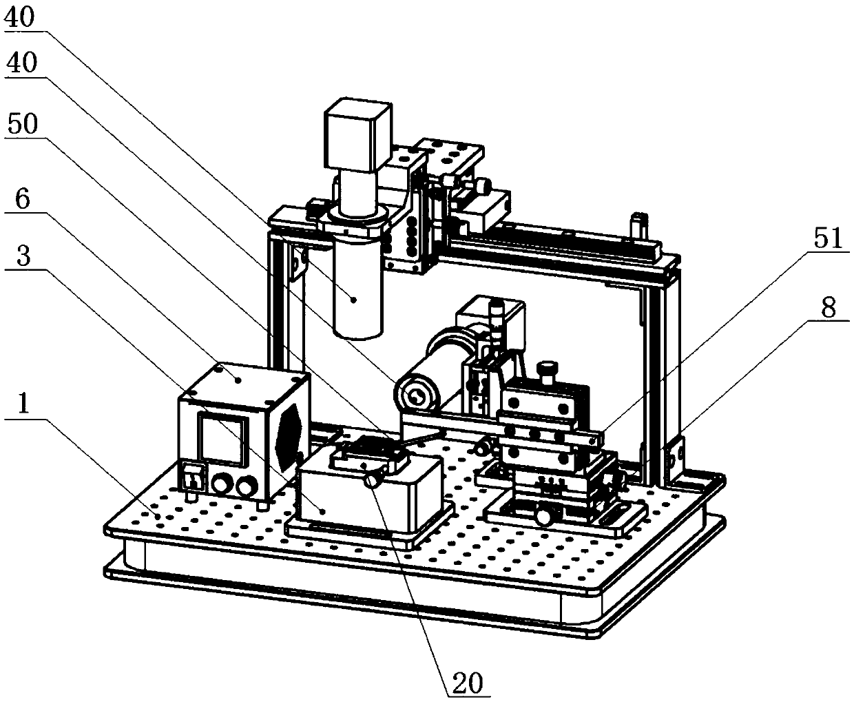
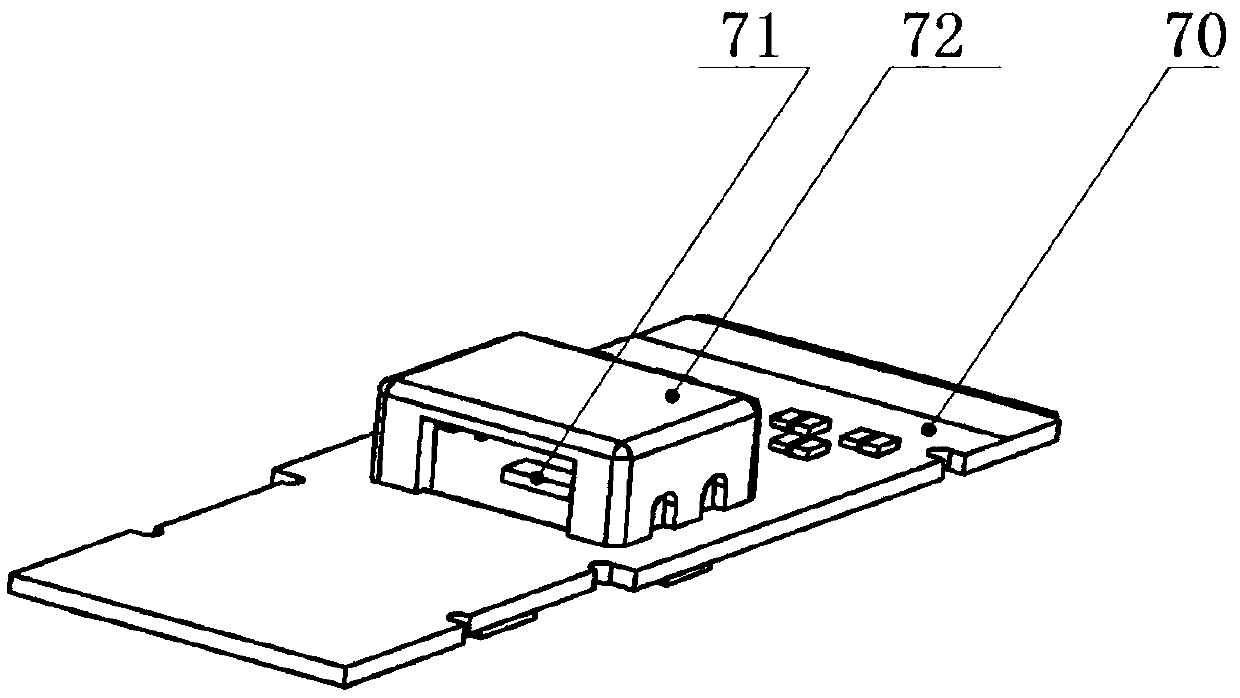
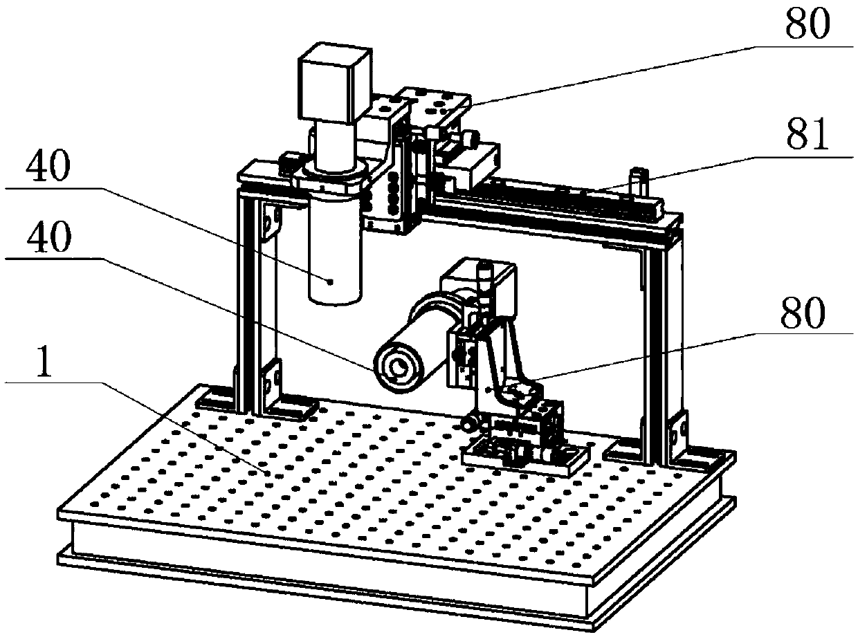
[0033] see figure 1 , the embodiment of the present invention provides a rework device for optical COB packaging, including a working platform, on which a fixing component 2, a heating component 3, an observation component and a stripping component are installed. Wherein, the fixing assembly 2 is used to fix the PCBA board 70 to reduce the curing degree between the PD chip 71 and the PCBA board 70; the heating assembly 3 is used to heat the PCBA board 70; Th...


PUM


Abstract

The invention relates to the technical field of optical communication and provides a reworking device for optical COB package. The device comprises a working platform on which a fixing component, a heating component, an observation component and a peeling component are installed. The fixing component is used for fixing a PCBA board, the heating component is used for heating the PCBA board, the observation component is used for monitoring the condition of the PCBA board in real time, and the peeling component is used for removing a PD chip that is heated and loosened on the PCBA board. According to the reworking device for optical COB package, the PCBA board fixed on the fixing component can be heated by the heating component, the heating can accelerate the molecular motion of glue betweenPD and PCBA to reduce the degree of curing between the PD chip and the PCBA board, so the PD chip is easily peeled from the PCBA board by the peeling component, the peeling process is observed in realtime under the observation component, the whole process is completed by mechanical components, which is more precise than pure manual, and the damage to chip components on the PCBA board is prevented.

Description

technical field [0001] The invention relates to the technical field of optical communication, in particular to a rework device for optical COB packaging. Background technique [0002] The full name of COB package is chip on board package (Chips on Board, COB), which is to adhere the bare chip to the interconnection substrate with conductive or non-conductive adhesive. The key (Wirebond) is combined to realize its signal transmission. [0003] A typical COB packaging model in the field of optical communication see figure 2 As shown, 1 is PD, 2 is LENS, and 3 is PCBA. In the production process, the PD and the PCBA are first bonded together through the die-bonding process, then the PD and the PCBA are wire bonded, and finally the LENS is coupled with the PD on the PCBA to realize the optical path and the electrical signal. transmission. [0004] During the production process, the coupling operation may damage the PD, or poor incoming materials may cause the coupled module t...

Claims


Application Information

Patent Timeline
IPC IPC(8): H05K13/04
CPCH05K13/0486
Inventor 程国锦李林科吴天书杨现文张健
Owner LINKTEL TECH CO LTD
Why Eureka
Try Eureka