Three-dimensional memory and manufacturing method thereof

A manufacturing method and memory technology, applied in semiconductor/solid-state device manufacturing, electric solid-state devices, semiconductor devices, etc., can solve problems such as poor performance of three-dimensional memory, meet the requirements of reducing flatness, improve production efficiency, and ensure performance.

Inactive Publication Date: 2019-03-29
YANGTZE MEMORY TECH CO LTD
View PDF2 Cites 20 Cited by
  • Summary
  • Abstract
  • Description
  • Claims
  • Application Information

AI Technical Summary

Problems solved by technology

[0005] The invention provides a three-dimensional memory and its manufacturing method, which are used to solve the problem of poor performance of the existing three-dimensional memory

Method used


Image

  • Three-dimensional memory and manufacturing method thereof
  • Three-dimensional memory and manufacturing method thereof
  • Three-dimensional memory and manufacturing method thereof

Examples


Embodiment Construction

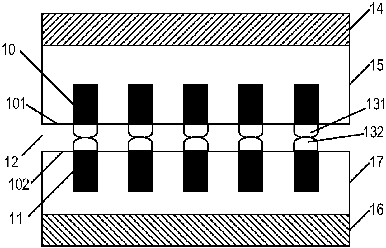
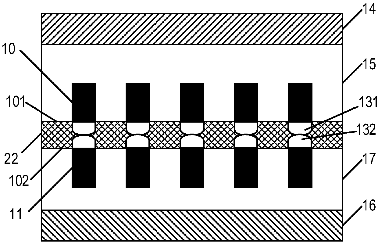
[0051] The specific implementation of the three-dimensional memory and its manufacturing method provided by the present invention will be described in detail below in conjunction with the accompanying drawings.

[0052] In the three-dimensional memory, the memory array wafer and the peripheral circuit wafer are electrically connected by bonding. Usually, the bonding of the memory array wafer and the peripheral circuit wafer is direct contact bonding between dielectric layers. The specific way of bonding the storage array wafer and the peripheral circuit wafer is: at a specific bonding temperature, the bonding surface of the storage array wafer is in contact with the bonding surface of the peripheral circuit, And use external pressure to bond the two wafers together.

[0053] However, this method of relying on the direct contact of the dielectric layers on the two wafers to achieve bonding has at least the following two defects: on the one hand, since the dielectric layers on ...


PUM


Abstract

The present invention relates to the technical field of semiconductor manufacturing, and especially relates to a three-dimensional memory and a manufacturing method thereof. The three-dimensional memory provided by the present invention comprises a first wafer having a first bonding surface and a first conductive layer exposed to the first bonding surface; a second wafer having a second bonding surface which is disposed to face the first bonding surface, and a second conductive layer exposed on the second bonding surface; a conductive bump which is located between the first bonding surface andthe second bonding surface and is electrically connected with the first conductive layer and the second conductive layer, wherein the first wafer and the second wafer are connected by at least the conductive bump. The connection strength between the first wafer and the second wafer is improved, and the performance of the three-dimensional memory is also improved.

Description

technical field [0001] The invention relates to the technical field of semiconductor manufacturing, in particular to a three-dimensional memory and a manufacturing method thereof. Background technique [0002] As technology develops, the semiconductor industry is constantly seeking new ways to produce a greater number of memory cells per memory die in a memory device. In non-volatile memory, such as NAND memory, one way to increase the memory density is by using vertical memory arrays, that is, 3D NAND (three-dimensional NAND) memory; 32 layers developed to 64 layers, or even higher layers. Xtacking type 3D NAND memory is currently a relatively cutting-edge three-dimensional memory technology with great development potential. [0003] In the Xtacking type 3D NAND memory, it usually includes peripheral device wafers and memory array wafers bonded to each other. However, due to the limitation of the existing technology, the performance of the bonded three-dimensional memory...

Claims


Application Information

Patent Timeline
Patent Type & Authority Applications(China)
IPC IPC(8): H01L23/48H01L21/60H01L27/11524H01L27/11551H01L27/1157H01L27/11578
CPCH01L24/81H01L23/48H01L2224/81H10B41/20H10B41/35H10B43/20H10B43/35
Inventor 刘峻
Owner YANGTZE MEMORY TECH CO LTD
Why Eureka
Try Eureka