
Liquid crystal display and manufacturing method thereof

A technology of a liquid crystal display and a manufacturing method, applied in the field of liquid crystal displays, can solve the problems of damage to display elements, incomplete curing of sealant, etc.

Inactive Publication Date: 2019-04-02
CHUNGHWA PICTURE TUBES LTD
View PDF5 Cites 2 Cited by
  • Summary
  • Abstract
  • Description
  • Claims
  • Application Information

AI Technical Summary

Problems solved by technology

However, during the process of separating the flexible substrate and the carrier substrate, the ultraviolet light used for separation may damage the display elements in the flexible display
On the other hand, the production process of some flexible displays involves the step of using ultraviolet light to cure the frame glue. However, since the ultraviolet light will pass through the flexible substrate and then irradiate the frame glue, the material of the flexible substrate will affect the UV light. The effect of curing the frame glue, some flexible displays will have the problem of incomplete curing of the frame glue

Method used


Image

  • Liquid crystal display and manufacturing method thereof
  • Liquid crystal display and manufacturing method thereof
  • Liquid crystal display and manufacturing method thereof

Examples


Embodiment Construction

[0024] The present invention will be further described in detail below in conjunction with the accompanying drawings and specific embodiments.

[0025] Although a series of operations or steps are used to illustrate the methods disclosed herein, the order in which these operations or steps are shown should not be construed as a limitation of the present invention. For example, certain operations or steps may be performed in a different order and / or concurrently with other steps. In addition, not all illustrated operations, steps and / or features must be performed to implement an embodiment of the invention. Furthermore, each operation or step described herein may contain several sub-steps or actions.

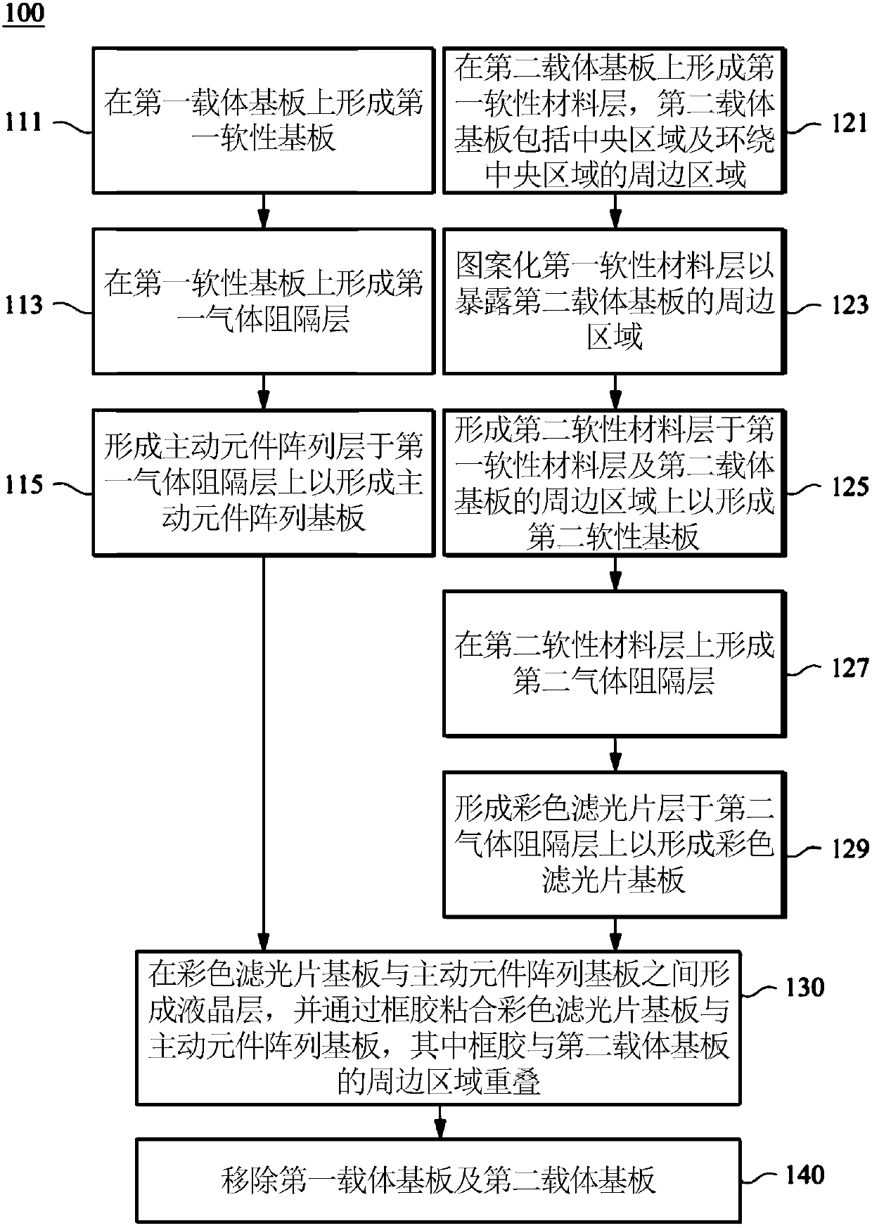
[0026] The invention provides a method for manufacturing a liquid crystal display, please refer to Figure 1 to Figure 11 . figure 1 is a flow chart of a method 100 for manufacturing a liquid crystal display according to some embodiments of the present invention. The method 10...


PUM

PropertyMeasurementUnit
wavelengthaaaaaaaaaa
transmittivityaaaaaaaaaa

Abstract

The invention discloses a liquid crystal display and a manufacturing method thereof. The liquid crystal display comprises a first flexible substrate, a display structure, a frame glue, and a second flexible substrate. The display structure is located on the first flexible substrate. The frame glue surrounds side surfaces of the display structure. The second flexible substrate is located on the frame glue and the display structure. One of the first flexible substrate and the second flexible substrate comprises a first flexible material layer and a second flexible material layer. The second flexible material layer is interposed between the first flexible material layer and the display structure, and part of the layer surrounds the side surfaces of the first flexible material layer and overlaps the frame glue. The ultraviolet light transmittance of the second flexible material layer is higher than the ultraviolet light transmittance of the first flexible material layer. In the process ofmanufacturing the liquid crystal display, the above structural design can make the curing degree of the frame glue to be good, when the frame glue is cured with ultraviolet light; and the above structural design can make the display structure not that easily damaged by the laser, and the lift-off yield is high, when the laser lift-off is performed.

Description

technical field [0001] The present invention relates to the field of display technology, in particular to a liquid crystal display (Liquid crystal display, LCD). Background technique [0002] In recent years, with the continuous development of display technology, a flexible display (Flexible display) has been developed in the field of display technology, which has the characteristics of thinness, flexibility and impact resistance, and has a wide range of applications. [0003] Generally speaking, the manufacturing method of the flexible display is to fix the flexible substrate on the carrier substrate first, and then manufacture the display elements on the flexible substrate. After the display element is manufactured and the flexible display is formed, the carrier substrate is removed. However, in the process of separating the flexible substrate and the carrier substrate, the ultraviolet light used for separation may damage the display elements in the flexible display. On ...

Claims


Application Information

Patent Timeline
Patent Type & Authority Applications(China)
IPC IPC(8): G02F1/1333G02F1/1339
CPCG02F1/1333G02F1/133305G02F1/1339G02F2202/28G02F1/133354H01L27/1218G02F1/133516G02F1/1368G02F2201/501G02F2203/01G02F2203/055G02F1/13398H01L27/1262
Inventor 陆文正黄彦馀郭哲成
Owner CHUNGHWA PICTURE TUBES LTD
Learn More