Semiconductor sensor and method for manufacturing same

A manufacturing method and semiconductor technology, applied in the direction of semiconductor/solid-state device manufacturing, semiconductor devices, semiconductor/solid-state device components, etc., can solve the problem of excessive film waste

Active Publication Date: 2019-04-02
DENSO CORP
View PDF6 Cites 2 Cited by
  • Summary
  • Abstract
  • Description
  • Claims
  • Application Information

AI Technical Summary

Problems solved by technology

Therefore, the film must be attached to the whole...

Method used


Image

  • Semiconductor sensor and method for manufacturing same
  • Semiconductor sensor and method for manufacturing same
  • Semiconductor sensor and method for manufacturing same

Examples


no. 1 Embodiment approach

[0045] Hereinafter, a first embodiment of the present invention will be described with reference to the drawings. The semiconductor sensor of this embodiment is configured as a physical quantity sensor such as a pressure sensor, a flow sensor, or an acceleration sensor, for example.

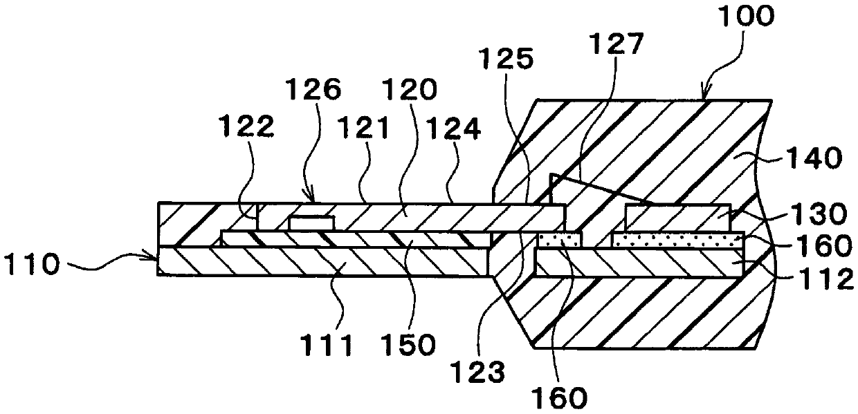
[0046] Such as figure 1 As shown, the semiconductor sensor 100 includes a lead frame 110 , a semiconductor chip 120 , a circuit chip 130 and a cast resin part 140 .

[0047] The lead frame 110 is a metal plate-shaped component, and functions as a fixing portion for the semiconductor chip 120 and the circuit chip 130 and as a terminal for electrically connecting the circuit chip 130 to the outside. The lead frame 110 has a first island 111 , a second island 112 , and a plurality of terminals not shown.

[0048] The first island portion 111 is a component on which the semiconductor chip 120 is mounted. The second island portion 112 is a component on which a part of the semiconductor chip 120 an...

no. 2 Embodiment approach

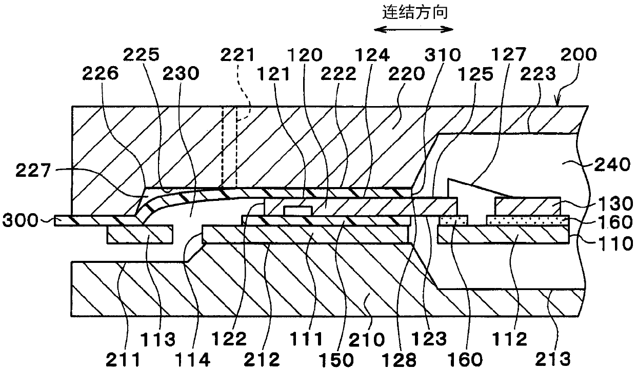
[0082] In this embodiment, differences from the first embodiment will be described. In this embodiment, in the preparatory process, such as Figure 14 As shown, an upper mold 220 having a protrusion 229 is prepared. The protruding portion 229 is a portion of the wall surface 225 of the upper mold 220 facing the gate portion 113 protruding from the step portion 222 facing the first island portion 111 .

[0083] and, if Figure 15 As shown, the resin molding process is performed using the upper mold 220 . The protruding portion 229 of the upper mold 220 makes the height of the space on the side of the gate portion 113 in the first space portion 230 lower than the height of the space on the side of the first island portion 111 . The height of the space corresponds to the width in the direction in which the lead frame 110 is sandwiched between the lower mold 210 and the upper mold 220 . Thus, if Figure 16 As shown, the thickness of the portion corresponding to the gate porti...


PUM


Abstract

Disclosed is a semiconductor sensor manufacturing method wherein an upper molding die (220) has a pair of protruding sections (224) so as to sandwich a semiconductor chip (120), the protruding sections being at positions closest to the second space (240) side in wall surface (225) portions facing side surfaces (122) of the semiconductor chip (120). Since gaps (231) between side surfaces (122) of the semiconductor chip (120) and the upper molding die (220) are narrowed by means of the pair of protruding sections (224), a flow of a resin material (143) from a first space (230) to a second space(240) can be slowed. Consequently, the first space (230) is filled with the resin material (143) before the second space (240), and the whole film (300) portion corresponding to the first space (230)is adhered to the upper molding die (220), then, the second space (240) is filled with the resin material (143).

Description

[0001] Cross-reference of related applications [0002] This application is based on Japanese Patent Application No. 2016-158534 filed on August 12, 2016, the contents of which are cited here. technical field [0003] The present invention relates to a semiconductor sensor and a manufacturing method thereof. Background technique [0004] For example, Patent Document 1 proposes a structure in which a semiconductor chip is covered with a cast resin portion so that a part of the semiconductor chip is exposed. This structure can be manufactured as follows. First, a semiconductor chip is prepared. In addition, a mold in which a space portion is formed by an upper mold and a lower mold is prepared. The upper mold has a protruding portion protruding from a portion of the upper mold corresponding to the periphery of the exposed portion of the semiconductor chip. [0005] Next, the film was affixed to the entire surface of the upper mold facing the lower mold. In addition, a sem...

Claims


Application Information

Patent Timeline
IPC IPC(8): B29C45/14B29C45/26H01L21/56
CPCH01L2924/181H01L2224/73265B29C45/0046B29C45/14655B29L2031/34B29L2031/752H01L21/565H01L23/3107H01L2924/00012H01L21/56B29C45/26B29C45/14065B29C45/17H01L23/49541
Inventor 田中昌明
Owner DENSO CORP
Why Eureka
Try Eureka