Substrate alignment method

A substrate and alignment marking technology, which is applied in optics, instruments, and photoplate-making processes on patterned surfaces, etc., can solve problems such as identification failure, interference with CCD identification effects, and impact on automatic production of products, so as to improve accuracy and success rate effect

Active Publication Date: 2019-04-05
TCL CHINA STAR OPTOELECTRONICS TECH CO LTD
View PDF3 Cites 0 Cited by
  • Summary
  • Abstract
  • Description
  • Claims
  • Application Information

AI Technical Summary

Problems solved by technology

[0005] The steps for aligning the glass substrate Mark and the mask Mark in the prior art are as follows: 1. Move the CCD to the top of the mask Mark; 2. Move the glass substrate Mark to directly below the mask Mark; In the same window, 4. The CCD focuses on the mask Mark for identification, 5. The CCD focuses on the glass substrate Mark for identification and positioning, and 6. The positions of the two Marks are combined for calculation; The glass substrate Mark is also made of metal, so it will also appear bright white after reflection. When the two Marks are aligned, they all appear bright white in the same window. When the CCD focuses on the mask Mark, it will be reflected by the lower glass substrate Mark. Influence, which seriously interferes with the recognition effect of CCD, resulting in failure of recognition, and manual alignment adjustment is required in the follow-up, which will seriously affect the automatic production of products

Method used


Image

  • Substrate alignment method
  • Substrate alignment method
  • Substrate alignment method

Examples


Embodiment Construction

[0029] In order to further illustrate the technical means adopted by the present invention and its effects, the following describes in detail in conjunction with preferred embodiments of the present invention and accompanying drawings.

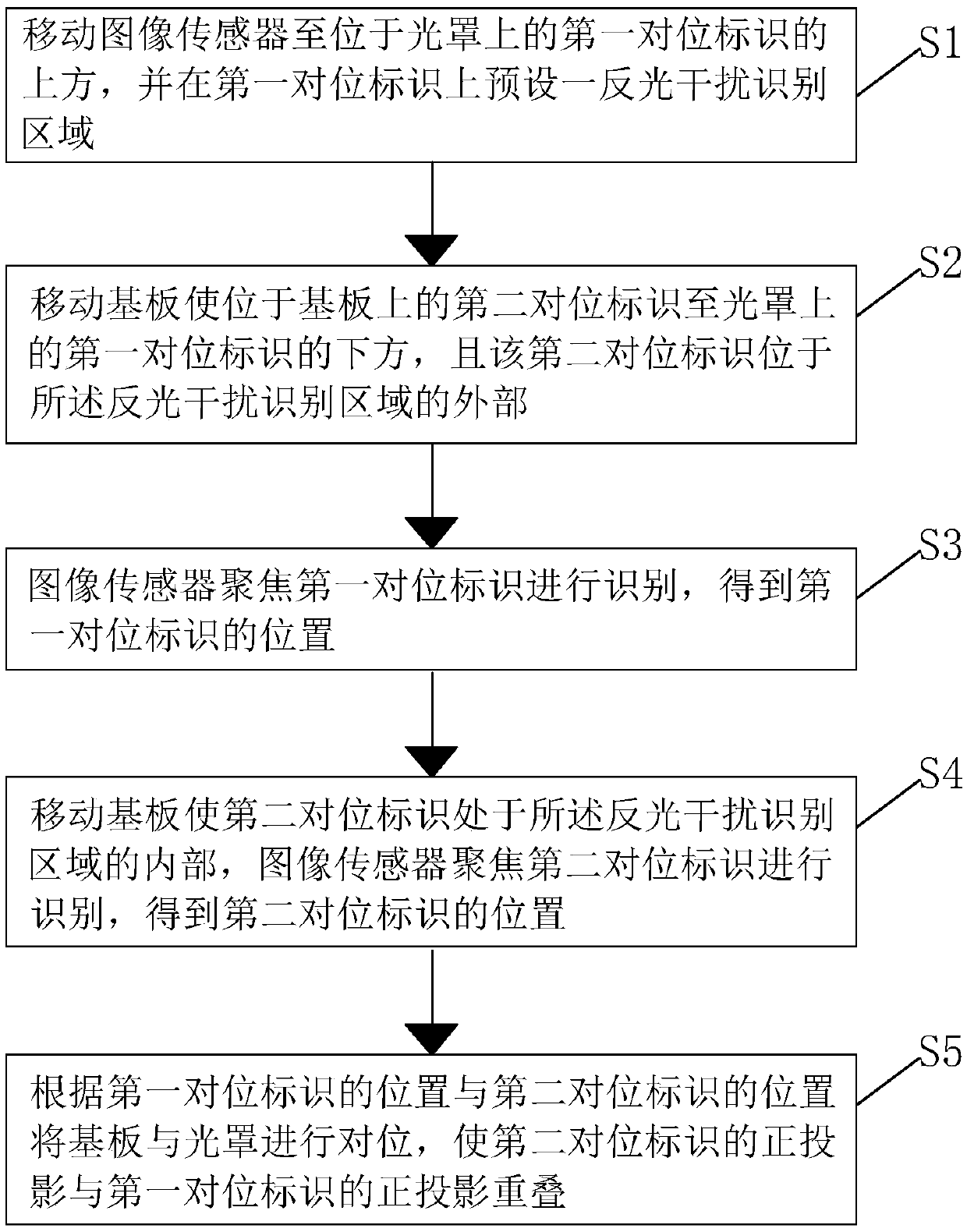
[0030] see figure 1 , the present invention provides a substrate alignment method, comprising the following steps:

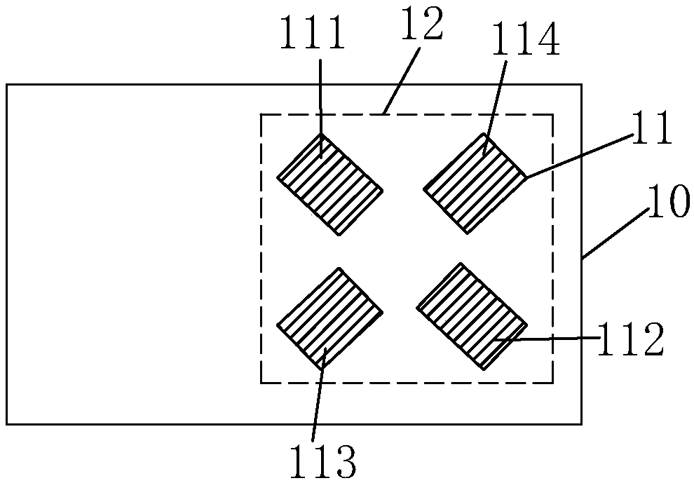
[0031] Step S1, please refer to figure 2 , move the image sensor to the top of the first alignment mark 11 located on the mask 10, and preset a reflective interference recognition area 12 on the first alignment mark 11;

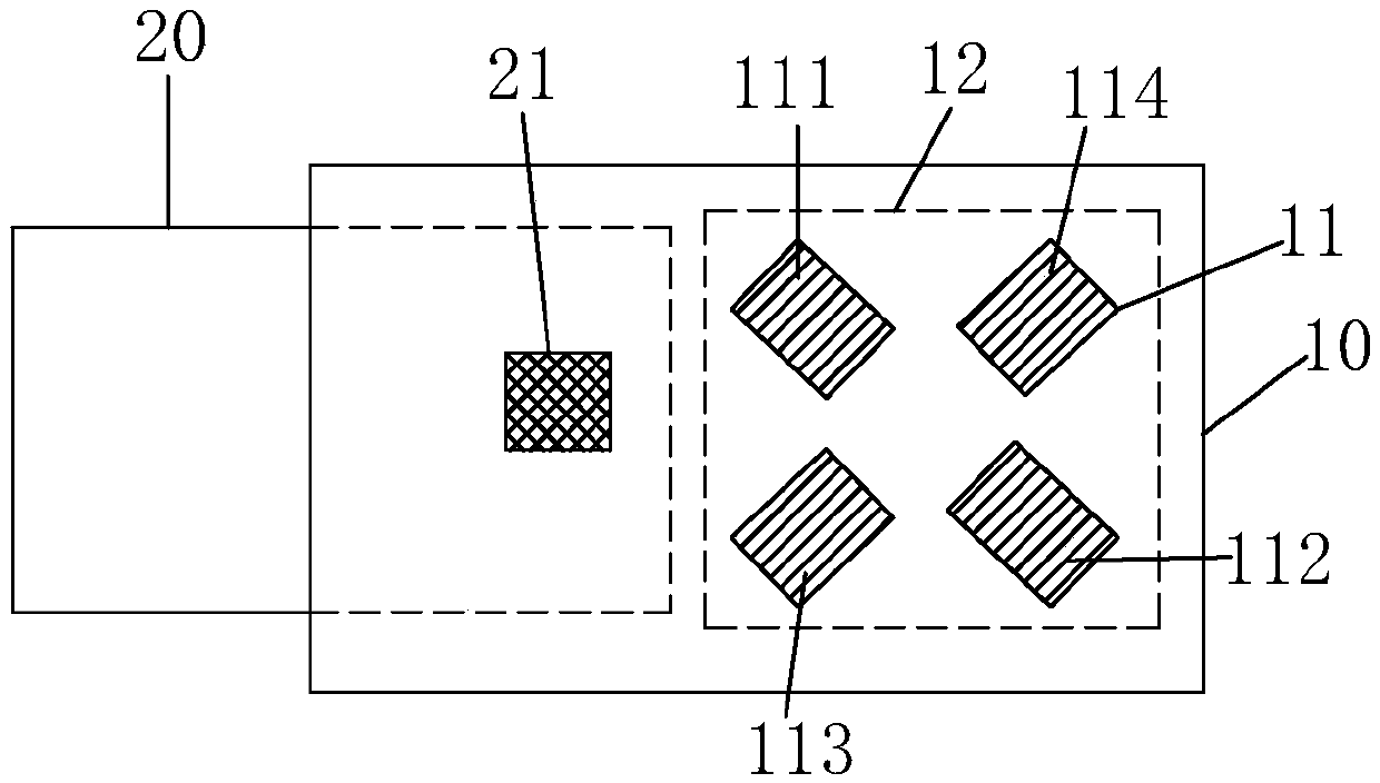
[0032] Step S2, please refer to image 3 , moving the substrate 20 so that the second alignment mark 21 located on the substrate 20 is below the first alignment mark 11 on the photomask 10, and the second alignment mark 21 is located outside the reflective interference identification area 12;

[0033] Step S3, the image sensor focuses on the first alignment mark 11 for identification, and obtains the positi...


PUM


Abstract

The invention provides a substrate alignment method. The substrate alignment method comprises pre-arranging a reflective interference recognition area on a first alignment mark on a photomask; movinga substrate in order that a second alignment mark on the substrate is below the first alignment mark and is located outside the reflective interference recognition area; enabling an image sensor to focus on the first alignment mark for recognition, wherein in the recognition process, the reflective interference of the second alignment mark can be avoided so as to accurately obtain the position ofthe first alignment mark. The method is not required to modify the structure of an alignment device, is just required to change the alignment logic of the alignment device to prevent the reflective interference of the second alignment mark on the substrate from affecting the accuracy of the alignment, and improves the accuracy and success rate of recognizing the first alignment mark on the photomask.

Description

technical field [0001] The invention relates to the field of display technology, in particular to a substrate alignment method. Background technique [0002] Thin Film Transistor (TFT) is the main driving element in current Liquid Crystal Display (LCD) and Active Matrix Organic Light-Emitting Diode (AMOLED). It is related to the display performance of the flat panel display device. [0003] Most of the liquid crystal displays currently on the market are backlight liquid crystal displays, which include a liquid crystal display panel and a backlight module. The working principle of the liquid crystal display panel is to pour liquid crystal molecules between the thin film transistor array substrate (ThinFilm Transistor Array Substrate, TFT Array Substrate) and the color filter (ColorFilter, CF) substrate, and apply pixel voltage on the two substrates respectively. and the common voltage, through the electric field formed between the pixel voltage and the common voltage to con...

Claims


Application Information

Patent Timeline
Patent Type & Authority Applications(China)
IPC IPC(8): G03F9/00G02F1/13
CPCG02F1/1303G03F9/7046G03F9/7088
Inventor 胡立巍叶人豪王载忠
Owner TCL CHINA STAR OPTOELECTRONICS TECH CO LTD
Why Eureka
Try Eureka