New-type enhanced semiconductor device and preparation method thereof

A semiconductor, enhancement-mode technology, used in semiconductor devices, semiconductor/solid-state device manufacturing, electrical components, etc., can solve the problem that the selective growth of p-GaN materials is difficult to control, the concentration of holes in the p-GaN layer is not high, and the quality of epitaxial crystals is affected. and other problems, to achieve the effect of high stability, reduced requirements, and high conduction capability

Active Publication Date: 2019-04-05
SUN YAT SEN UNIV
View PDF6 Cites 6 Cited by
  • Summary
  • Abstract
  • Description
  • Claims
  • Application Information

AI Technical Summary

Problems solved by technology

However, due to the influence of epitaxial growth kinetics, when the gate length of the device is small, that is, when the growth window is very narrow, the selective growth of p-GaN materials is difficult to control and the doping is uneven. There is currently no breakthrough in these areas.
Moreover, selective growth requires the formation of an additional patterned mask layer on the wafer surface, the most commonly used is SiO 2 mask layer, SiO at high temperature 2 It is easy to decompose to produce Si and O elements, which diffuse into the epitaxial layer and easily form donor doping, which leads to leakage and seriously affects the quality of the epitaxial crystal, and the influence of the mask layer on the epitaxial growth kinetics cannot be ignored
In addition, the hole concentration of the p-GaN layer is generally not high, and the current mainstream reported value is basically no higher than 1×10 18 cm -3 , so the Al composition of the AlGaN barrier layer under the p-GaN layer is generally required to be less than 20% and the thickness is less than 18nm, which is conducive to the realization of enhanced operation, but at the same time it will lead to an increase in the resistance of the access region, and the relatively thin The AlGaN barrier layer will also make it easier for the dopant elements (such as magnesium) in the p-type GaN layer to diffuse into the channel, thereby affecting the reliability of the device

Method used


Image

  • New-type enhanced semiconductor device and preparation method thereof
  • New-type enhanced semiconductor device and preparation method thereof
  • New-type enhanced semiconductor device and preparation method thereof

Examples


Embodiment 1

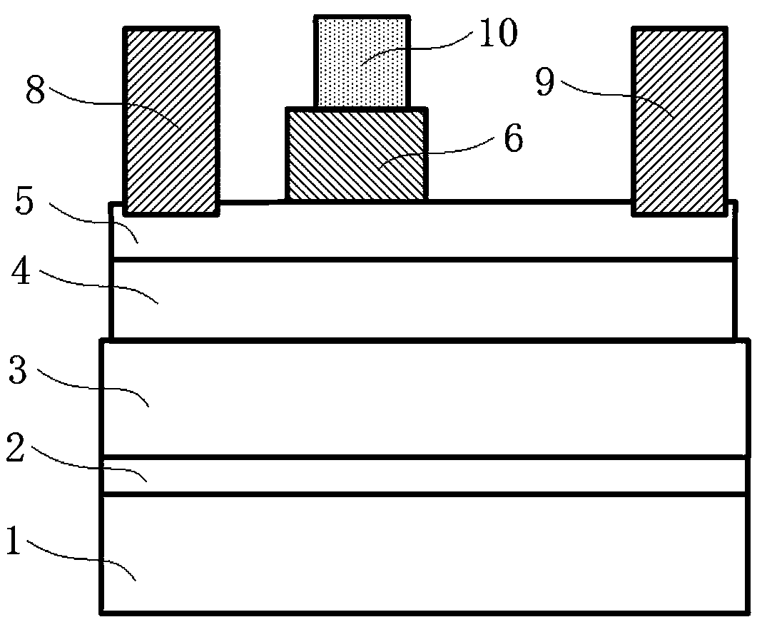
[0055] Such as Figure 12 Shown is a schematic diagram of the device structure of this embodiment, a semiconductor enhancement transistor, including a substrate 1 , a semiconductor epitaxial layer grown on the substrate 1 , a gate 10 , a source 8 and a drain 9 . The epitaxial layer includes, from bottom to top, a nitride nucleation layer 2, a nitride stress buffer layer 3, a nitride channel layer 4, a primary epitaxial nitride barrier layer 5, and a p-type nitride layer 6 and a secondary epitaxial layer. Nitride barrier layer 7 . The p-type nitride layer 6 remains only on the primary epitaxial nitride barrier layer 5 in the region of the gate 10 to realize the pinch-off of the two-dimensional electron gas channel under the gate 10 . The secondary epitaxy has no mask, and the secondary epitaxial nitride barrier layer 7 is grown on the primary epitaxial barrier layer and the p-type nitride layer 6 in the region of the gate 10 .

[0056] The fabrication method of the above-ment...

Embodiment 2

[0070] Such as Figure 13 Shown is a schematic diagram of the device structure of this embodiment, which differs from the structure of Embodiment 1 only in that a layer of AlN space is sandwiched between the nitride channel layer 4 and the primary epitaxial nitride barrier layer 5 in Embodiment 2. The isolation layer 11 has a thickness of 0.3-3 nm. It is used to improve the two-dimensional electron gas characteristics of the channel.

Embodiment 3

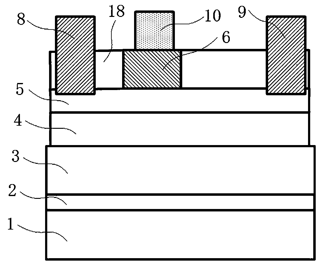
[0072] Such as Figure 14 Shown is a schematic diagram of the device structure of this embodiment, which differs from the structure of Embodiment 1 only in that: Embodiment 1 is middle, and part of the primary epitaxial nitride barrier layer 5 outside the gate 10 region is removed, while Embodiment 3 Part of the primary epitaxial nitride barrier layer 5 outside the region of the middle gate 10 remains intact. Compared with Example 1, Example 3 requires a harsher etching scheme, such as more advanced equipment, or self-terminating etching conditions containing oxygen or fluorine.


PUM

PropertyMeasurementUnit
thicknessaaaaaaaaaa
thicknessaaaaaaaaaa
thicknessaaaaaaaaaa

Abstract

The invention relates to a new-type enhanced semiconductor device and a preparation method thereof. The new-type enhanced semiconductor device comprises a substrate, a semiconductor epitaxial layer, agate, a source, and a drain. The semiconductor epitaxial layer comprises a nitride nucleation layer, a nitride stress buffer layer, a nitride channel layer, a primary epitaxial nitride barrier layer,a p-type nitride layer, and a secondary epitaxial nitride barrier layer. Through etching, the p-type nitride in a gate region is retained to achieve pinch-off of the gate channel. Through the mask-less secondary epitaxy, the secondary epitaxial nitride barrier layer is grown on the primary epitaxial barrier layer and a p-type nitride layer in the gate region to realize a high conduction accessingregion. The secondary epitaxy can effectively repair etch damage, and the requirements for the etching process are also reduced. Through adjusting and controlling the thickness and composition of theprimary epitaxial nitride barrier layer and the secondary epitaxial nitride barrier layer, better gate turn-off and accessing region conduction capability can be achieved. The invention can realize an enhanced semiconductor device with high threshold voltage, high conduction, high stability and low leakage.

Description

technical field [0001] The invention relates to the technical field of semiconductor devices, and more specifically, relates to a novel enhanced semiconductor device and a preparation method thereof. Background technique [0002] The third-generation semiconductor materials represented by GaN materials have great room for development in high-temperature, high-frequency, radiation-resistant, and high-power applications due to their advantages such as wide bandgap, high thermal conductivity, and high breakdown electric field. [0003] GaN-based electronic devices usually use the two-dimensional electron gas with high concentration and high mobility at the interface of AlGaN / GaN heterostructure to work, so that the device has the advantages of small on-resistance, large output current, and fast switching speed. However, it is precisely because of this AlGaN / GaN heterostructure (high two-dimensional electron gas, 2DEG) that the device is naturally turned on when the external gat...

Claims


Application Information

Patent Timeline
Patent Type & Authority Applications(China)
IPC IPC(8): H01L29/778H01L21/335
CPCH01L29/66462H01L29/7786H01L29/1066H01L29/2003H01L29/402H01L29/41766H01L29/42316H01L29/401
Inventor 刘扬何亮
Owner SUN YAT SEN UNIV
Why Eureka
Try Eureka