Diamond-based normally-off type field effect transistor and preparation method therefor

A field-effect transistor, diamond technology, applied in transistors, semiconductor/solid-state device manufacturing, semiconductor devices and other directions, can solve the problems affecting device performance and carrier mobility, etc., to improve safety and energy saving. Effect

Active Publication Date: 2017-07-25
XI AN JIAOTONG UNIV
View PDF2 Cites 11 Cited by
  • Summary
  • Abstract
  • Description
  • Claims
  • Application Information

AI Technical Summary

Problems solved by technology

This technology is to dope a high concentration of impurities in a very thin layer inside the diamond, but this technology has a great impact on the carrier mobility, which in turn affects the device performance

Method used


Image

  • Diamond-based normally-off type field effect transistor and preparation method therefor
  • Diamond-based normally-off type field effect transistor and preparation method therefor
  • Diamond-based normally-off type field effect transistor and preparation method therefor

Examples


Embodiment

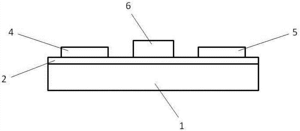
[0080] A method for preparing a diamond-based normally-off field-effect transistor comprises the following steps:

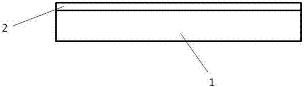
[0081] Step 1. Clean the diamond substrate 1 using a standard acid-base cleaning process to remove the non-diamond phase on the surface, then clean the diamond substrate 1 with alcohol, acetone, and deionized water, and dry the diamond substrate 1 with nitrogen gas. .

[0082] Step 2, growing a single crystal diamond epitaxial film 2 on the diamond substrate 1 by microwave plasma chemical vapor deposition technology. The growth conditions are: power 1KW, chamber pressure 50Torr, total gas flow 500sccm.

[0083] After the growth in step 3 and step 2 is completed, the plasma is turned off, the chamber pressure is kept constant, and only hydrogen gas is introduced to realize hydrogenation of the surface of the single crystal diamond epitaxial film 2 .

[0084] Step 4. Clean the hydrogenated sample with alcohol, acetone and deionized water respectively, and dry the...


PUM


Abstract

The invention discloses a diamond-based normally-off type field effect transistor. The diamond-based normally-off type field effect transistor comprises a diamond substrate, wherein a monocrystal diamond epitaxial thin film is arranged on the diamond substrate; an active region and a device isolation device which surrounds the active region are arranged on the surface of the monocrystal diamond epitaxial thin film; the active region comprises two-dimensional hole gas; a source, a gate and a drain are arranged above the active region in sequence; conductive channels are formed in the surface of the active region; the conductive channels comprise the channels with alternately arranged hydrogen terminals and oxygen terminals, or alternately arranged hydrogen terminals and fluorine terminals; the oxidization or fluorination degree of the conductive channels are adjusted through a surface processing technology, so that depletion degree of the hydrogen terminal parts close to the oxygen terminals or the fluorine terminals can be further adjusted, so as to realize the switch-off characteristic of a gate bias zero device; and the normally-off type device which can be widely applied in the fields of high voltage and high frequency electronics can be provided.

Description

[0001] 【Technical field】 [0002] The invention belongs to the field of semiconductor devices, in particular to a diamond-based normally-off field effect transistor and a preparation method thereof. [0003] 【Background technique】 [0004] In people's production and life, semiconductor devices play an increasingly important role. The single crystal material for manufacturing semiconductor devices has also experienced four generations of development. As one of the representatives of the fourth-generation semiconductor materials, diamond has excellent properties unmatched by other semiconductor materials. In terms of electricity, diamond has a high band gap, ultra-high breakdown voltage, high Johnson index, high Keyes index, high Baliga index, large electron mobility and hole mobility. Therefore, ultra-high-frequency and ultra-high-power electronic devices made of diamond materials have inherent advantages, and their performance can also surpass the previous three generations o...

Claims


Application Information

Patent Timeline
Patent Type & Authority Applications(China)
IPC IPC(8): H01L29/778H01L29/10H01L21/335
CPCH01L29/1054H01L29/66045H01L29/778
Inventor 王宏兴王艳丰王玮常晓慧李硕业张景文卜忍安侯洵
Owner XI AN JIAOTONG UNIV
Why Eureka
Try Eureka