Diode structure and fabrication method based on Gan-based heterostructure

A technology of heterogeneous structure and manufacturing method, applied in semiconductor/solid-state device manufacturing, electrical components, circuits, etc., can solve the problem of increasing the forward voltage drop of the device, high turn-on voltage, difficult low turn-on voltage and low reverse Leakage work and other problems to achieve the effect of improving blocking characteristics and low turn-on voltage

Active Publication Date: 2017-01-11
INST OF SEMICONDUCTORS - CHINESE ACAD OF SCI
View PDF3 Cites 0 Cited by
  • Summary
  • Abstract
  • Description
  • Claims
  • Application Information

AI Technical Summary

Problems solved by technology

However, due to the high barrier height formed by the Schottky junction and the band step between heterostructures, diodes with this structure tend to have a higher turn-on voltage, thereby increasing the forward voltage drop of the device.
The use of Schottky metal with low work function will bring about the problem of high reverse leakage. It is difficult to achieve low turn-on voltage and low reverse leakage at the same time using traditional methods.

Method used


Image

  • Diode structure and fabrication method based on Gan-based heterostructure
  • Diode structure and fabrication method based on Gan-based heterostructure

Examples


Embodiment Construction

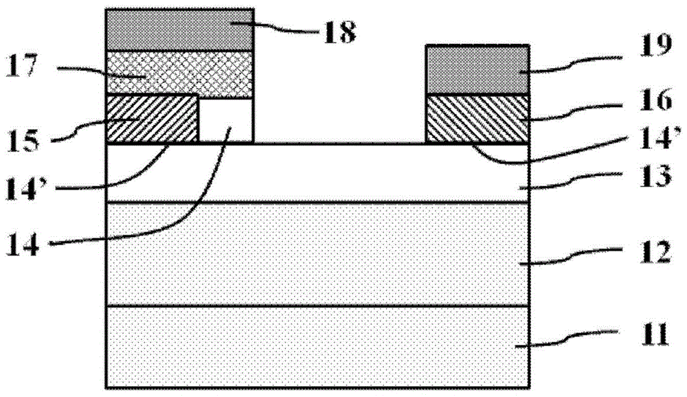
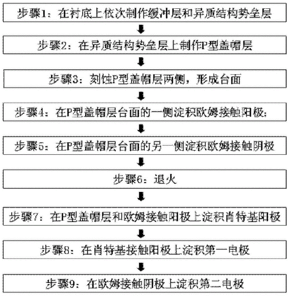
[0034] see figure 1 As shown, the present invention provides a diode based on a GaN-based heterostructure, comprising:

[0035] A substrate 11, the material of the substrate 11 is sapphire, silicon carbide, diamond, gallium nitride, or silicon substrate, etc., its thickness is 1 μm-1cm, and the doping concentration is 1×10 10 -1×10 23 cm -3 ;

[0036] A buffer layer 12, which is made on the substrate 11, the material of the buffer layer 12 is GaN, AlGaN or AlN, or any combination of one or more layers of GaN, AlGaN or AlN, and its thickness is 1nm -10μm, the doping concentration is 1×10 10 -1×10 23 cm -3 , the buffer layer 12 reduces the lattice mismatch between the substrate and the epitaxial layer, improves the crystal quality of the epitaxial layer, and simultaneously reduces device leakage;

[0037] A heterostructure barrier layer 13, which is fabricated on the buffer layer 12, forms a heterostructure epitaxial layer of two-dimensional electron gas with the buffer l...


PUM


Abstract

A diode based on a GaN-based heterostructure comprises a substrate, a buffer layer, a heterostructure barrier layer, a heterostructure epitaxial layer, a P-type cap layer, an ohmic contact anode, an ohmic contact cathode, a Schottky anode, a first electrode and a second electrode. The buffer layer is manufactured on the substrate, the heterostructure barrier layer is manufactured on the buffer layer, the heterostructure epitaxial layer and the buffer layer form two-dimensional electron gas, the P-shaped cap layer is manufactured on the heterostructure barrier layer, table faces are formed on the two sides of the P-type cap layer, the ohmic contact anode is manufactured on the heterostructure barrier layer, and is located close to the table face on one side, the ohmic contact cathode is manufactured on the heterostructure barrier layer and on the table face on the other side far away from the P-type cap layer, the Schottky anode is manufactured on the P-type cap layer and the ohmic contact anode, the first electrode is manufactured on the Schottky anode, and the second electrode is manufactured on the ohmic contact cathode. According to the diode, the starting voltage of a device can be lowered, and meanwhile device low reverse electric leakage and high barrier feature working can be achieved.

Description

technical field [0001] The invention relates to the technical field of semiconductors, in particular to a GaN-based heterostructure-based diode and a manufacturing method. Background technique [0002] Gallium nitride (GaN), a wide bandgap semiconductor material, has the characteristics of wide bandgap, high critical breakdown electric field strength, high saturation electron drift velocity, small dielectric constant and good chemical stability, especially GaN-based materials. The heterojunction structure has high electron mobility and high two-dimensional electron gas concentration, which makes GaN-based devices have low on-resistance and high operating frequency, which can meet the needs of next-generation electronic equipment for higher power and higher power devices. Frequency, smaller volume and harsher high-temperature work requirements have broad application prospects in civilian and military fields. With the advancement of GaN technology, especially the gradual matu...

Claims


Application Information

Patent Timeline
Patent Type & Authority Patents(China)
IPC IPC(8): H01L29/872H01L21/329
CPCH01L29/0684H01L29/452H01L29/475H01L29/66143H01L29/872
Inventor 康贺王晓亮肖红领王翠梅冯春姜丽娟殷海波崔磊
Owner INST OF SEMICONDUCTORS - CHINESE ACAD OF SCI
Why Eureka
Try Eureka