Hetetrostructure field effect diode and manufacturing method thereof

A technology of field-effect diodes and heterostructures, applied in semiconductor/solid-state device manufacturing, electrical components, circuits, etc., can solve difficult problems such as low conduction voltage and low reverse leakage current

Inactive Publication Date: 2011-06-15
SUN YAT SEN UNIV
View PDF5 Cites 14 Cited by
  • Summary
  • Abstract
  • Description
  • Claims
  • Application Information

AI Technical Summary

Problems solved by technology

Therefore, it is difficult to achieve low turn-on voltage and low reverse

Method used


Image

  • Hetetrostructure field effect diode and manufacturing method thereof
  • Hetetrostructure field effect diode and manufacturing method thereof
  • Hetetrostructure field effect diode and manufacturing method thereof

Examples


Embodiment 1

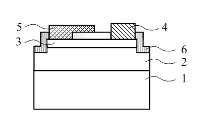
[0034] figure 1 It is a schematic structural diagram of an AlGaN / GaN heterojunction field effect diode according to the first embodiment of the present invention.

[0035] Such as figure 1 As shown, the substrate 1 can be sapphire Sapphire, silicon Si, silicon carbide SiC, gallium nitride GaN, gallium arsenide GaAs substrate, etc. Located on the substrate 1 is a high-resistance GaN layer 2, which may be a doped or non-doped layer or a combination of layers, with a thickness between 200 nanometers and 10 microns. Located on the high-resistance GaN layer 2 is an AlGaN barrier layer 3 with a thickness between 2-50 nanometers. A 2DEG channel is formed between the AlGaN barrier layer 3 and the high-resistance GaN layer 2, and the concentration is 10 10 -10 14 / cm 2 between.

[0036] The insulating dielectric layer 6 located on the AlGaN barrier layer 3, the insulating dielectric layer 6 has at least one layer of insulating material with a high dielectric constant, and the thi...

Embodiment 2

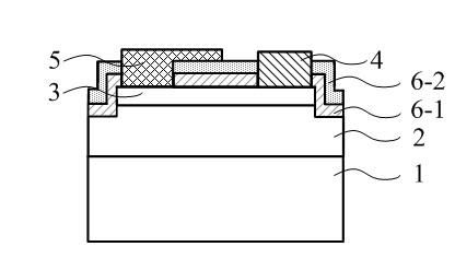
[0040] figure 2 It is a schematic structural diagram of an AlGaN / GaN heterojunction field effect diode in the second example of the present invention.

[0041] The structure in this embodiment is basically the same as that in Embodiment 1, the difference is that: a structure of two insulating dielectric layers 6 is adopted, wherein layer 6-1 is a low dielectric constant material, and layer 6-2 is a material with a higher dielectric constant Material.

[0042] The first layer of the insulating dielectric layer adopts a low dielectric constant dielectric layer 6-1, which is SiO in this embodiment 2 , and the thickness is between 2-10 nanometers, the purpose is to optimize and improve the quality of the growth interface of the insulating dielectric layer; the second layer adopts the high dielectric constant dielectric layer 6-2, and selects Al in this embodiment 2 o 3 , with a thickness of 5-20 nm. The purpose of selecting the dielectric layer 6-2 with high dielectric consta...

Embodiment 3

[0044] The present invention also provides a method for manufacturing a heterostructure field effect diode, which includes the following steps:

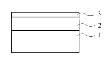
[0045] A. As shown in FIG. 3( a ), there are substrate 1 , insulating high-resistance semiconductor 2 , and wide-gap heterostructure barrier layer 3 in sequence.

[0046] B. As shown in FIG. 3( b ), after the pattern of the active region is formed by photolithography, an isolation mesa is formed by etching to realize electrical isolation of the active region.

[0047] C. As shown in Figure 3(c), one or more layers of insulating dielectric layer 6 are deposited on the isolation table, and the number of layers and the thickness of each layer can be adjusted according to needs;

[0048] D. As shown in Figure 3(d), the electrode pattern is first photoetched on the table by photolithography, and then the insulating dielectric layer 6 is etched to form a window for electrode evaporation by dry or wet etching. For the next step to evaporat...


PUM

PropertyMeasurementUnit
Thicknessaaaaaaaaaa
Lengthaaaaaaaaaa
Thicknessaaaaaaaaaa

Abstract

The invention discloses a hetetrostructure field effect diode and a manufacturing method thereof. The hetetrostructure field effect diode comprises a substrate as well as an insulation high-resistance semiconductor and a wide bandgap hetetrostructure barrier layer which are sequentially arranged on the substrate, wherein the insulation high-resistance semiconductor and the wide bandgap hetetrostructure barrier layer form a two-dimensional electron gas hetetrostructure epitaxial layer, an isolated table board is formed at the top of the insulation high-resistance semiconductor and the wide bandgap hetetrostructure barrier layer, an insulating medium layer is formed on the isolated table board, a cathode electrode and an anode electrode which are contacted with the wide bandgap hetetrostructure barrier layer are respectively formed on the insulating medium layer, wherein one part of the anode electrode is arranged on the wide bandgap hetetrostructure barrier layer, the other part of the anode electrode is arranged on the insulating medium layer to form a diode anode provided with a Schottky-MIS (metal-insulator-semiconductor) dual-structure electrode, and the anode electrode is made from a low-work function metal. According to the invention, the characteristics of low forward on voltage, low reverse leakage current and high reverse blocking voltage can be realized, thus, the method in the invention is applicable to manufacturing of a power type GaN-base hetetrostructure field effect diode.

Description

technical field [0001] The invention belongs to the field of power semiconductor devices, and in particular relates to a heterogeneous structure field effect diode and a manufacturing method. Background technique [0002] As an indispensable part of voltage regulators, rectifiers, and inverters, power Schottky diodes are used more and more in daily life, mainly involving high-voltage power supply, power management, factory automation, and motor vehicle energy distribution. management and many other fields. At the same time, as power Schottky diodes are more and more widely used in the field of power electronics, higher and higher requirements are placed on their performance. [0003] Current power Schottky diodes mainly use Si-based materials. However, due to the limitations of material characteristics such as the bandgap width and electron mobility of Si materials, the performance of silicon-based power devices is close to its theoretical limit, which cannot meet today's ...

Claims


Application Information

Patent Timeline
IPC IPC(8): H01L29/861H01L29/06H01L29/40H01L29/417H01L21/329
Inventor 刘扬邓庆煜姚尧
Owner SUN YAT SEN UNIV
Why Eureka
Try Eureka