Quantum resistance standard device

A standard device and resistance technology, applied in the field of quantum resistance standard devices, can solve the problems affecting the high-accuracy transmission and use of resistance units, extremely demanding and complicated operations, and achieve the effect of promoting and applying.

Pending Publication Date: 2019-04-09
NAT INST OF METROLOGY CHINA
View PDF0 Cites 2 Cited by
  • Summary
  • Abstract
  • Description
  • Claims
  • Application Information

AI Technical Summary

Problems solved by technology

However, the reproduction of quantum Hall resistance is extremely demanding on the environment. Quantum resistance needs to be reproduced under extremely low temperature and strong magnetic field. At present, the traditional method of commercial superconducting magnet + sample probe + quantum Hall resistance chip is adopted in the world. Quantum resistance reproduction provides a low temperature and strong magnetic field environment, which is bulky (most national resistance benchmark laboratories provide a separate room for it), and the operation is extremely complicated (involving cooling, excitation, and sample probe operation at the same time), and it is difficult for personnel to operate. The technical requirements are high, and the operation time can even be as long as a few days. Therefore, in the past 40 years since the emergence of quantum resistance, only national and regional laboratories have the ability and conditions to enable and maintain the natural reference device of quantum Hall resistance, and then through the physical resistance test. The multi-level chain is delivered to the user, and the maximum uncertainty when it is delivered to the user is only 10 -7 order of magnitude, which seriously affects the transfer and use of resistance units with high accuracy
To sum up, the complexity, personnel requirements, and work efficiency of the quantum Hall resistance value reproduction device severely limit its wide-scale promotion and application. All aspects of production and life

Method used


Image

  • Quantum resistance standard device
  • Quantum resistance standard device

Examples


Embodiment

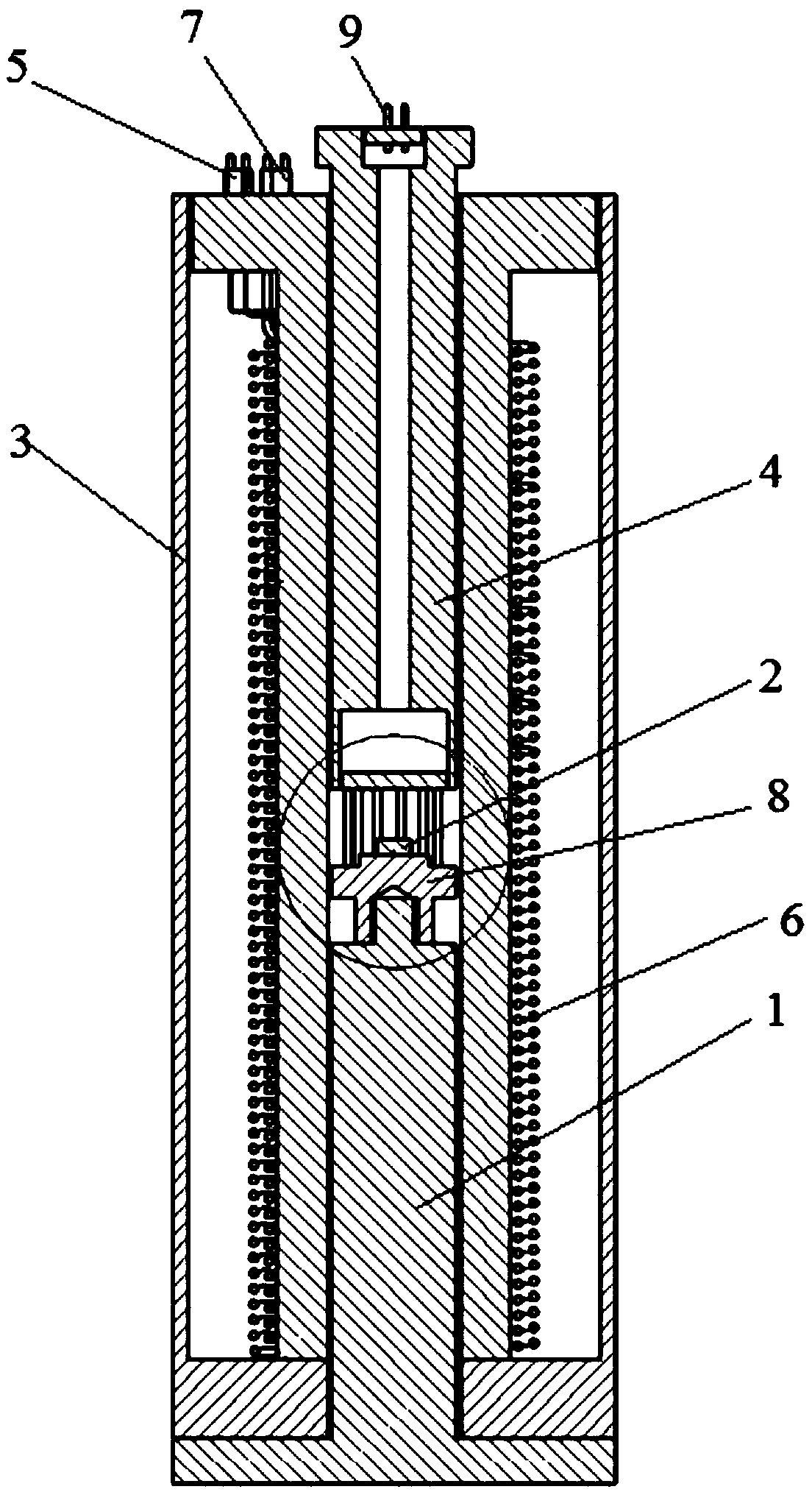
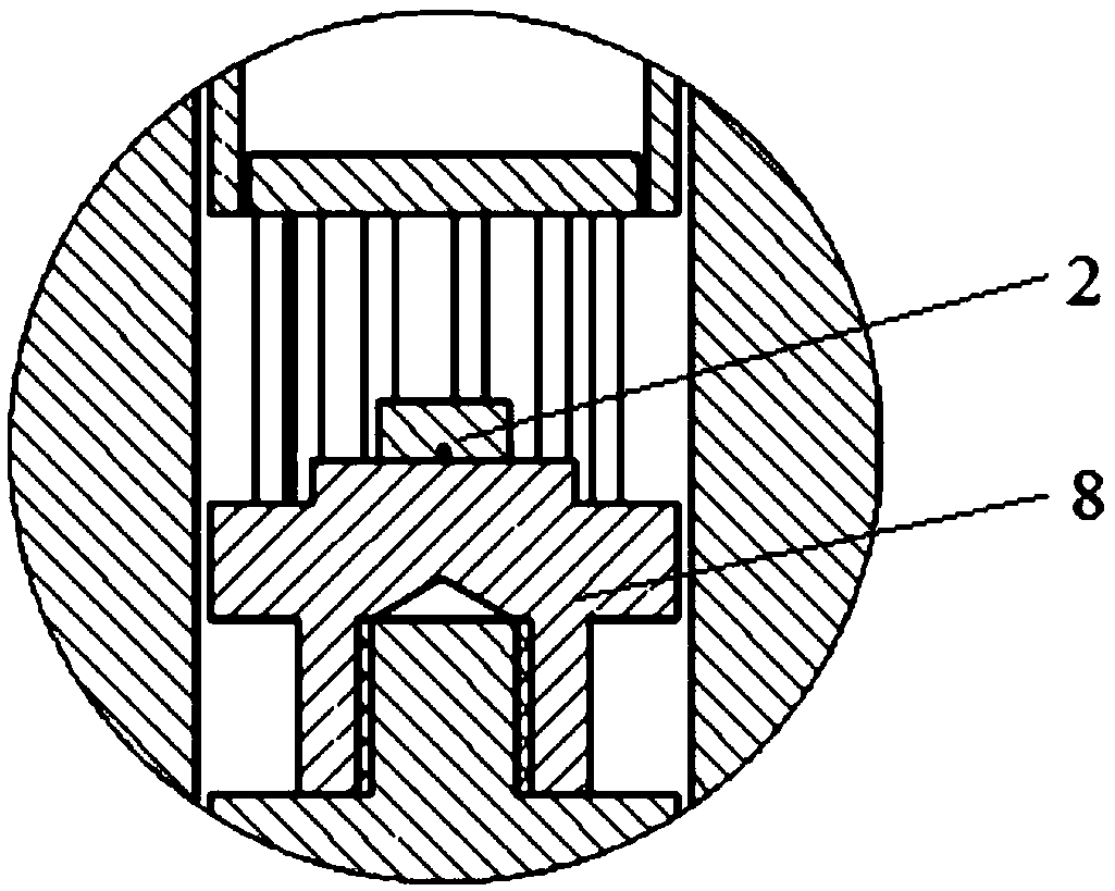
[0052] figure 1 A schematic structural diagram of a quantum resistance standard according to an embodiment of the present invention is shown. figure 2 A schematic structural diagram showing the installation position of the quantum Hall resistance chip of the quantum resistance standard according to an embodiment of the present invention.

[0053] like Figure 1-Figure 2 As shown, the quantum resistance standard includes:

[0054] A superconducting coil, the superconducting coil includes a hollow tubular thermally conductive skeleton 4 and a superconducting wire 6 wound outside the thermally conductive skeleton 4, the quantum Hall resistance chip 2 is arranged inside the thermally conductive skeleton 4, when When the superconducting wire 6 is energized, a magnetic field can be generated in the thermally conductive skeleton 4;

[0055] A heat conduction mechanism 2, one end of the heat conduction mechanism 2 is connected to the quantum Hall resistance chip 3;

[0056] Metal...


PUM


Abstract

The invention provides a quantum resistance standard device. The quantum resistance standard device comprises a superconducting solenoid coil, a quantum hall resistance chip, a heat conduction mechanism and a metal shell, wherein the quantum hall resistance chip is arranged in the superconducting solenoid coil; when the superconducting solenoid coil is electrified, the quantum hall resistance chipis located in a magnetic field; one end of the heat conduction mechanism is connected to the quantum hall resistance chip; and the metal shell is buckled on the superconducting solenoid coil and theheat conduction mechanism, and the other end of the heat conduction mechanism extends out of the metal shell. The quantum resistance standard device is small in size, convenient to use, easy to achieve working requirements and beneficial to popularization and application.

Description

technical field [0001] The invention belongs to the field of precision electrical measurement, and more specifically relates to a quantum resistance standard. Background technique [0002] According to the suggestion of the International Committee of Metrology CIPM, starting from January 1, 1990, the DC quantized Hall resistance benchmark was used worldwide, which opened the era of quantization of electromagnetic measurement. The reproduction of the resistance unit no longer depends on the physical resistance, but It is reproduced by quantized Hall resistance, and its accuracy has been improved by 2 to 3 orders of magnitude, and there is no need to worry about the drift, damage and international consistency of the actual resistance. my country built a quantized Hall resistance standard device in 2003, and its standard uncertainty reached 2.4×10 -10 . However, the reproduction of quantum Hall resistance is extremely demanding on the environment. Quantum resistance needs to ...

Claims


Application Information

Patent Timeline
Patent Type & Authority Applications(China)
IPC IPC(8): G01R1/20
CPCG01R1/203
Inventor 鲁云峰赵建亭贺青戴银明
Owner NAT INST OF METROLOGY CHINA
Why Eureka
Try Eureka