Supercharge Your Innovation With Domain-Expert AI Agents!

Deep trench isolation structure of cmos image sensor and its manufacturing method

A deep trench isolation, image sensor technology, applied in semiconductor devices, electric solid state devices, radiation control devices, etc., can solve the problems of low potential well capacity, inability to extend, isolation, etc., to increase the area and reduce the width. Effect

Active Publication Date: 2021-03-12
POWERCHIP SEMICON MFG CORP
View PDF7 Cites 0 Cited by
  • Summary
  • Abstract
  • Description
  • Claims
  • Application Information

AI Technical Summary

Problems solved by technology

[0003] Due to the limitations of the manufacturing process of the existing DTI, when the pixel size (pixel size) is reduced, its width still occupies a considerable device area
However, such a width makes the area of ​​the light-sensing region relatively reduced, resulting in a lower potential well capacity (full well capacity, FWC)
[0004] In addition, a common crystal back-side DTI in the prior art cannot extend to the front surface, so it cannot achieve complete isolation, especially for the crosstalk between long-wavelength light and charges
In addition, when forming the back-end DTI, in order to avoid the components formed on the front side of the chip in the back-end manufacturing process (BEOL) from being affected by high temperature, when forming the back-end DTI, for example, the annealing in the passivation step must be The temperature when controlling the heat transfer to the metal wiring of the BEOL is below 400°C, so it becomes difficult to control the heat source input from the crystal back, and it is difficult to achieve the purpose of high temperature activation of DTI surface doping

Method used


Image

  • Deep trench isolation structure of cmos image sensor and its manufacturing method
  • Deep trench isolation structure of cmos image sensor and its manufacturing method
  • Deep trench isolation structure of cmos image sensor and its manufacturing method

Examples


Embodiment Construction

[0063]Some embodiments are listed below and described in detail with the accompanying drawings, but the provided embodiments are not intended to limit the scope of the present invention. In addition, the drawings are for illustration purposes only and are not drawn to original scale. In order to facilitate understanding, the same elements in the following description will be described with the same symbols. In addition, terms such as "comprising", "including", and "having" used in the text are all open terms; that is, including but not limited to. Moreover, the directional terms mentioned in the text, such as: "up", "down", etc., are only used to refer to the directions of the drawings. Accordingly, the directional terms used are for the purpose of description, not limitation of the invention.

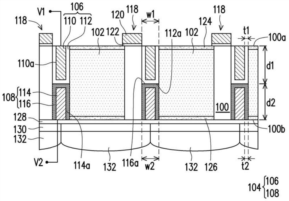
[0064] figure 1 is a schematic cross-sectional view of a CMOS image sensor (CIS) including a deep trench isolation structure (DTI) according to the first embodiment of the present i...


PUM

PropertyMeasurementUnit
thicknessaaaaaaaaaa

Abstract

The invention discloses a deep trench isolation structure of a CMOS image sensor and a manufacturing method thereof. The deep trench isolation structure includes a plurality of isolation structures located between photosensitive regions in a substrate, and each isolation structure It includes a first trench isolation structure and a second trench isolation structure. The first trench isolation structure is formed in the first surface of the substrate, wherein the first trench isolation structure includes a first filling layer and a first dielectric liner covering the surface of the first filling layer. The second trench isolation structure is formed in the second surface of the substrate opposite to the first surface, and the second trench isolation structure includes a second filling layer and a second dielectric liner covering the surface of the second filling layer, wherein The bottom surface of the second dielectric liner is in direct contact with the bottom surface of the first dielectric liner.

Description

technical field [0001] The present invention relates to a complementary metal oxide semiconductor image sensor (CMOS image sensor, CIS) technology, and in particular to a deep trench isolation structure (deep trench isolation, DTI) of a CMOS image sensor and its Manufacturing method. Background technique [0002] The deep trench isolation structure in the CMOS image sensor is used to isolate the light and charge between the CMOS image sensors, so as to reduce the crosstalk between the light and the charge between pixels. [0003] Due to the limitations of the manufacturing process of the conventional DTI, when the pixel size (pixel size) is reduced, its width still occupies a considerable device area. However, such a width makes the area of ​​the photo-sensing region relatively reduced, resulting in a lower full well capacity (FWC). [0004] In addition, a common back side DTI in the prior art cannot extend to the front surface, so it cannot achieve complete isolation, esp...

Claims


Application Information

Patent Timeline
Patent Type & Authority Patents(China)
IPC IPC(8): H01L27/146
CPCH01L27/1463H01L27/14683
Inventor 李世平王美文黄彬杰
Owner POWERCHIP SEMICON MFG CORP
Features
  • R&D
  • Intellectual Property
  • Life Sciences
  • Materials
  • Tech Scout
  • Unparalleled Data Quality
  • Higher Quality Content
  • 60% Fewer Hallucinations
Learn More