Light emitting diode package structure

A light-emitting diode and packaging structure technology, which is applied in the direction of electrical components, circuits, semiconductor devices, etc., can solve the problems of affecting the luminous efficiency, the accumulated heat cannot be dissipated, and the excitation degree of the phosphor powder of the light-emitting diode is different, so as to achieve uniform emission ability, Prevent light source attenuation and avoid the effect of uneven illumination range

Active Publication Date: 2019-04-16
合肥市华宇半导体有限公司
View PDF4 Cites 2 Cited by
  • Summary
  • Abstract
  • Description
  • Claims
  • Application Information

AI Technical Summary

Problems solved by technology

[0002] When the light-emitting diode is working, as the working time prolongs, a certain amount of heat is generated inside the package. Because the package in the prior art is completely sealed, th...

Method used


Image

  • Light emitting diode package structure
  • Light emitting diode package structure

Examples


Embodiment Construction

[0027] In order to make the technical means, creative features, goals and effects achieved by the present invention easy to understand, the technical solutions in the embodiments of the present invention will be clearly and completely described below in conjunction with the accompanying drawings in the embodiments of the present invention. Obviously, the The described embodiments are only some, not all, embodiments of the present invention. Based on the embodiments of the present invention, all other embodiments obtained by persons of ordinary skill in the art without creative efforts fall within the protection scope of the present invention.

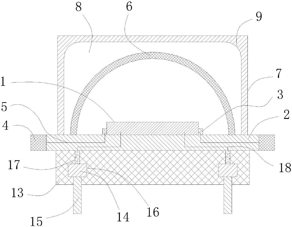
[0028] like Figure 1-2 The shown package structure of a light emitting diode includes the crystal 1 of the light emitting diode, and also includes:

[0029] base 2;

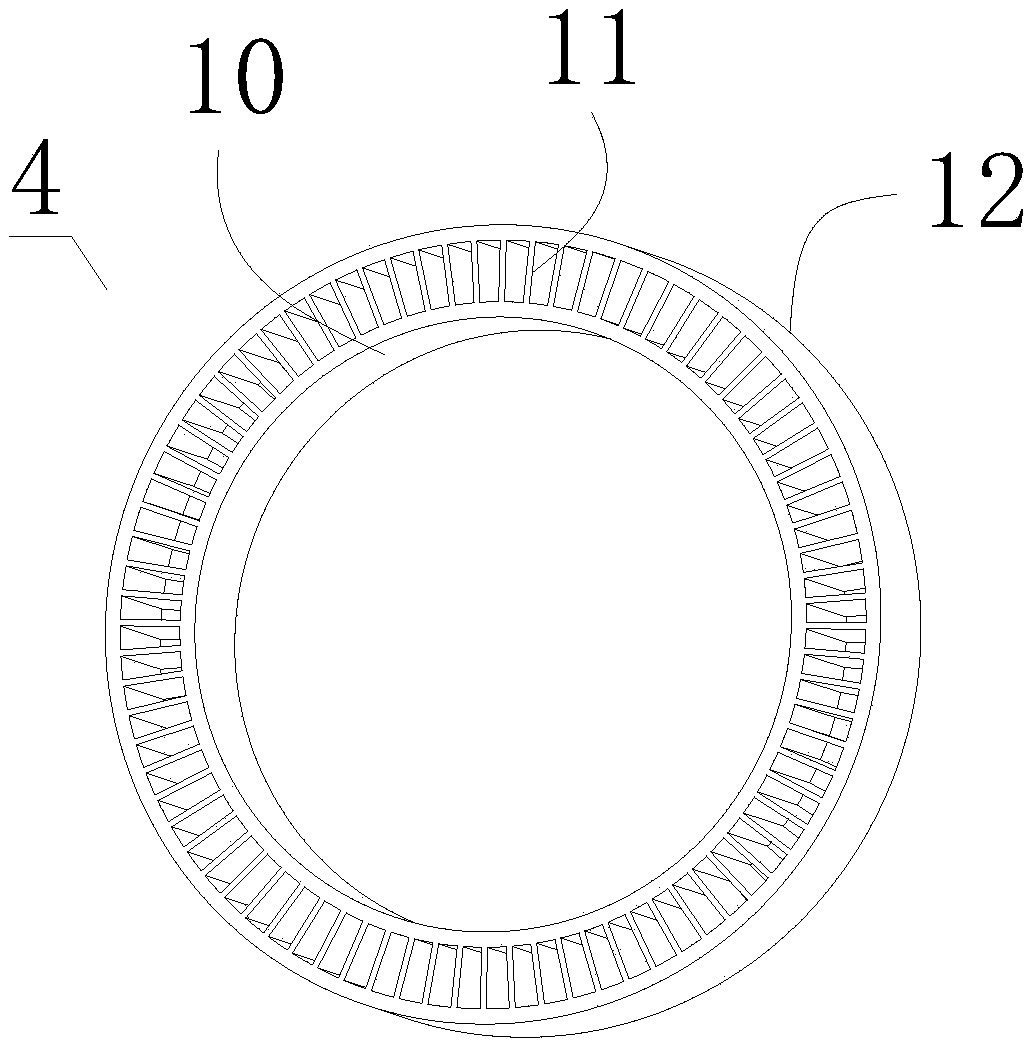
[0030] A fixed ring 3, the fixed ring 3 is arranged on the top of the base 2, and the crystal 1 is engaged on the middle hole of the fixed ring 3;

[0031] A heat diss...


PUM


Abstract

The invention relates to the technical field of light emitting diodes, in particular to a light emitting diode package structure. The light emitting diode package structure includes a crystal of a light emitting diode and further comprises a base, a fixing ring, a heat dissipating assembly, a heat dissipating wire, a lens and a transparent frame. The light emitting diode package structure is provided with the heat dissipating assembly, the fixing ring and the heat dissipating wire, heat generated by working of the light emitting diode is transmitted to the heat dissipating wire through the fixing ring, then the heat is transmitted to the heat dissipating assembly through the heat dissipating wire to realize timely heat dissipation of the crystal, and therefore the influence on the stimulating effect of phosphor powder coated on the crystal is avoided; the heat dissipating assembly consists of a clamping ring, heat dissipating fins and a connecting ring assembly, and the heat can be quickly dissipated through the heat dissipating fins; the lens is arranged, so that a light source emitted by the light emitting diode can be diffused through the lens to maximize the light emitting range; and meanwhile, hemispherical setting allows for uniform distribution of light throughout the lens, and uneven illumination range is avoided.

Description

technical field [0001] The invention relates to the technical field of light emitting diodes, in particular to a packaging structure of light emitting diodes. Background technique [0002] When the light-emitting diode is working, as the working time prolongs, a certain amount of heat is generated inside the package. Because the package in the prior art is completely sealed, the accumulated heat cannot be dissipated. To a certain extent, the coating inside the light-emitting diode The degree of excitation of the phosphor varies, which in turn affects the luminous efficiency. Contents of the invention [0003] The object of the present invention is to overcome the problems existing in the prior art and provide a light emitting diode packaging structure, which can dissipate the heat in the light emitting diode in time and avoid affecting the luminous efficiency. [0004] In order to achieve the above-mentioned technical purpose and achieve the above-mentioned technical effe...

Claims


Application Information

Patent Timeline
IPC IPC(8): H01L33/48H01L33/58H01L33/62H01L33/64
CPCH01L33/483H01L33/58H01L33/62H01L33/642
Inventor 彭勇
Owner 合肥市华宇半导体有限公司
Why Eureka
Try Eureka