Check patentability & draft patents in minutes with Patsnap Eureka AI!

AMOLED display panel

A display panel and display unit technology, applied in the direction of semiconductor devices, electrical components, circuits, etc., can solve the problem of the wide bottom of the AMOLED display panel, and achieve the effect of reducing the occupied area and width

Active Publication Date: 2019-04-23
WUHAN CHINA STAR OPTOELECTRONICS SEMICON DISPLAY TECH CO LTD
View PDF3 Cites 4 Cited by
  • Summary
  • Abstract
  • Description
  • Claims
  • Application Information

AI Technical Summary

Problems solved by technology

[0007] The embodiment of the present application provides an AMOLED display panel with a narrow frame; to solve the technical problem of the existing AMOLED display panel having a large bottom width

Method used


Image

  • AMOLED display panel
  • AMOLED display panel
  • AMOLED display panel

Examples


Embodiment Construction

[0052] Please refer to the drawings in the accompanying drawings, wherein like reference numerals refer to like components. The following description is based on illustrated specific embodiments of the present application, which should not be construed as limiting other specific embodiments of the present application that are not described in detail here.

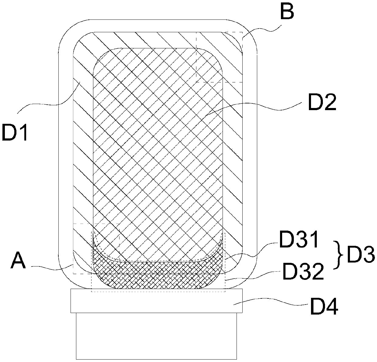
[0053] Please refer to image 3 , image 3 It is a schematic structural diagram of the first embodiment of the AMOLED display panel of the present application.

[0054] The AMOLED display panel of the first embodiment includes a drive circuit area D2 for driving the display light-emitting area D1 to emit light, a fan-out area D3 for setting fan-out lines, and a driver circuit area D2 and a fan-out area D3. The light emitting area D1 and the bending area D4 where bending is performed are shown.

[0055] The area of ​​the driving circuit area D2 is smaller than that of the display light emitting area D1, and the display li...


PUM


Abstract

The present application provides an AMOLED display panel. The AMOLED display panel comprises a display light-emitting area, and a drive circuit area and a fan-out area which are arranged at the lowerportion of the display light-emitting area, the area of the drive circuit area is smaller than the area of the display light-emitting area, and the display light-emitting area completely covers the drive circuit area and at least part of the fan-out area. The AMOLED display panel shortens the area of the lower edge area of the drive circuit area to save a certain space to set the wiring of the fan-out area so as to reduce the width o the lower margin of the display panel.

Description

technical field [0001] The present application relates to a display technology, in particular to an AMOLED display panel. Background technique [0002] With the development of display industry technology, customers have higher and higher requirements for display panels. For example, for some high-end display panels, customers will require narrow bezel design. [0003] With the development of flexible AMOLED display panels, a new Pad bending (area bending) technology is proposed to solve the problem of large lower borders of rigid panels. Bend the Bonding Pad (binding area) of the COF or the IC bonding pad area of ​​the COP under the existing display panel, and the fanout (fan-out) line connected to the Data signal in the pixel circuit of the AA area and some test circuit areas. Folding to the bottom of the panel can reduce the lower border of the original rigid display panel, as shown in the attached figure 1 shown. [0004] However, as attached figure 1 The schematic di...

Claims


Application Information

Patent Timeline
IPC IPC(8): H01L27/32
CPCH10K59/123H10K59/12H10K59/131
Inventor 孙亮王硕晟曾勉易士娟
Owner WUHAN CHINA STAR OPTOELECTRONICS SEMICON DISPLAY TECH CO LTD
Features
  • R&D
  • Intellectual Property
  • Life Sciences
  • Materials
  • Tech Scout
  • Unparalleled Data Quality
  • Higher Quality Content
  • 60% Fewer Hallucinations
Learn More