
Pixel driving circuit and driving method, display panel

A pixel driving circuit and driving method technology, applied in static indicators, instruments, etc., can solve the problems of low color depth of OLED and inability to adjust the light-emitting time of light-emitting devices, and achieve the effect of solving color depth

Active Publication Date: 2020-11-03
GIGADISPLAY SEMICON CO LTD
View PDF9 Cites 0 Cited by
  • Summary
  • Abstract
  • Description
  • Claims
  • Application Information

AI Technical Summary

Problems solved by technology

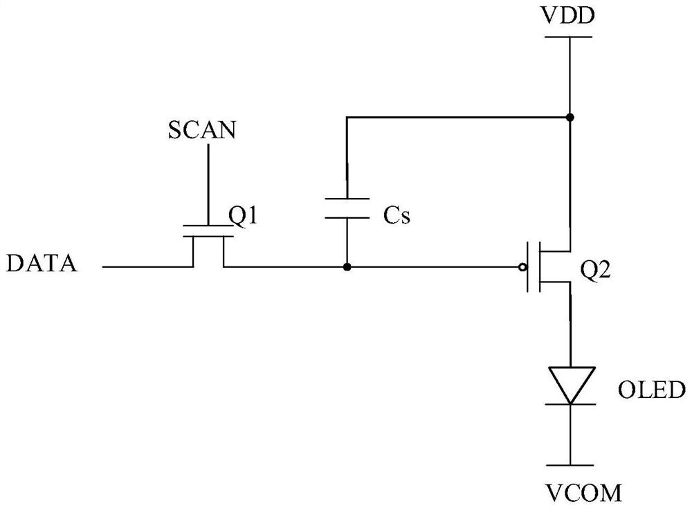
[0005] However, the pixel drive circuit in the prior art still has the following technical defects: the prior art cannot adjust the light-emitting time of the light-emitting device, and is limited by the accuracy of the gamma circuit in the case of low brightness, and the color depth of OLED is lower than that of normal brightness.

Method used


Image

  • Pixel driving circuit and driving method, display panel
  • Pixel driving circuit and driving method, display panel
  • Pixel driving circuit and driving method, display panel

Examples


Embodiment Construction

[0028] In order to facilitate the understanding of the present invention, the present invention will be described more fully below with reference to the associated drawings. Preferred embodiments of the invention are shown in the accompanying drawings. However, the present invention can be implemented in different forms and is not limited to the embodiments described herein. On the contrary, these embodiments are provided to make the understanding of the disclosure of the present invention more thorough and comprehensive.

[0029] Unless otherwise defined, all technical and scientific terms used herein have the same meaning as commonly understood by one of ordinary skill in the technical field of the invention. The terms used herein in the description of the present invention are for the purpose of describing specific embodiments only, and are not intended to limit the present invention.

[0030] Hereinafter, the present invention will be described in detail with reference t...


PUM


Abstract

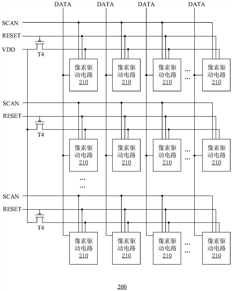
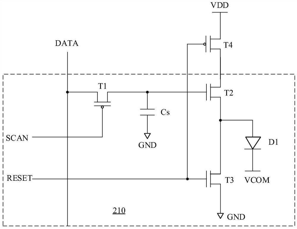
The invention discloses a pixel driving circuit, a driving method and a display panel. The pixel driving circuit comprises a first transistor whose turn-on and turn-off are controlled by a scan signal; a storage capacitor which is used for receiving the data voltage through the first transistor and storing the data voltage; a second transistor that supplies a driving voltage or a driving current to an anode of the light emitting element according to the power supply voltage and the stored data voltage in a turn-off phase of the first transistor; And a third transistor providing a current pathbetween the anode of the light emitting element and the reference ground, the on and off of the third transistor being controlled by a reset signal, the third transistor being turned on by the reset signal for a predetermined time during the off phase and / or on phase of the first transistor to release the anode charge of the light emitting element. The pixel driving circuit can release residual charges at the high potential end of the pixel driving circuit in the initialization stage and / or the light emitting stage of the light emitting element, so that the light emitting brightness can be controlled by controlling the light emitting time, and the smear problem is solved.

Description

technical field [0001] The invention relates to the field of display technology, in particular to a pixel driving circuit, a driving method, and a display panel. Background technique [0002] Silicon-based organic light-emitting diode (Organic Light-Emitting Diode on Silicon, OLED-on-Silicon) display device uses organic light-emitting diodes as light-emitting devices, and uses complementary metal oxide semiconductors as switching components or driving components of organic light-emitting diodes, including pixels Driving circuit, scanning driving circuit and necessary control circuit. Organic light-emitting diodes have many advantages such as simple process, low-voltage drive, low power consumption, low cost, high response speed, self-illumination, and wide viewing angle. [0003] Such as figure 1 As shown, a conventional voltage-type two-tube pixel driving circuit is taken as an example, and the pixel driving circuit includes: an organic light emitting diode OLED, transist...

Claims


Application Information

Patent Timeline
Patent Type & Authority Patents(China)
IPC IPC(8): G09G3/3291G09G3/3233
CPCG09G3/3233G09G3/3291G09G2320/0233
Inventor 孙丽娜田琪邢晓荣
Owner GIGADISPLAY SEMICON CO LTD
Learn More