
Connecting structure and circuit

A technology for connecting structures and circuits, applied in circuits, printed circuits, printed circuits, etc., can solve problems such as output signal degradation, and achieve the effect of suppressing the reduction of solderable areas

Active Publication Date: 2019-05-03
NEC CORP
View PDF8 Cites 0 Cited by
  • Summary
  • Abstract
  • Description
  • Claims
  • Application Information

AI Technical Summary

Problems solved by technology

[0004] On the other hand, it has been explained that the presence of the stub leads to degradation of a predetermined output signal (see Patent Documents 1 and 2)

Method used


Image

  • Connecting structure and circuit
  • Connecting structure and circuit
  • Connecting structure and circuit

Examples


Embodiment Construction

[0036]

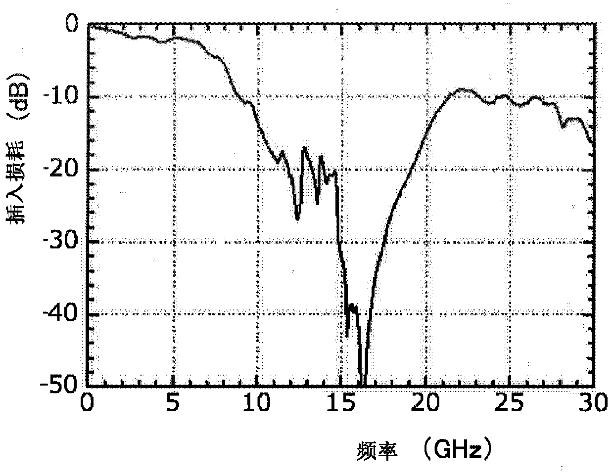
[0037] First, the effect of the stub of a pair of vias with a capacitor placed on the output has been examined.

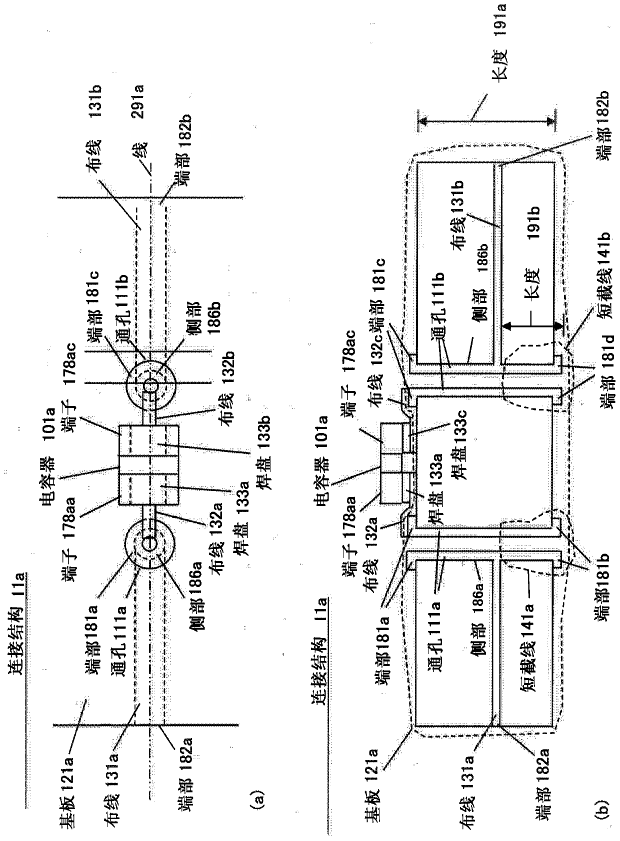
[0038] figure 1 is a conceptual diagram illustrating the configuration of the connection structure 11a used in this study. figure 1 (a) is a top view of the connection structure 11a. figure 1 (b) assumes that the connection structure 11a is figure 1 (a) Cross-sectional view cut by indicated line 291a.

[0039] The connection structure 11a includes a substrate 121a, a capacitor 101a, wirings 132a and 132c, and pads 133a and 133c.

[0040] The substrate 121a includes wirings 131a and 131b and through holes 111a and 111b. The thickness of the substrate 121a is the length 191a.

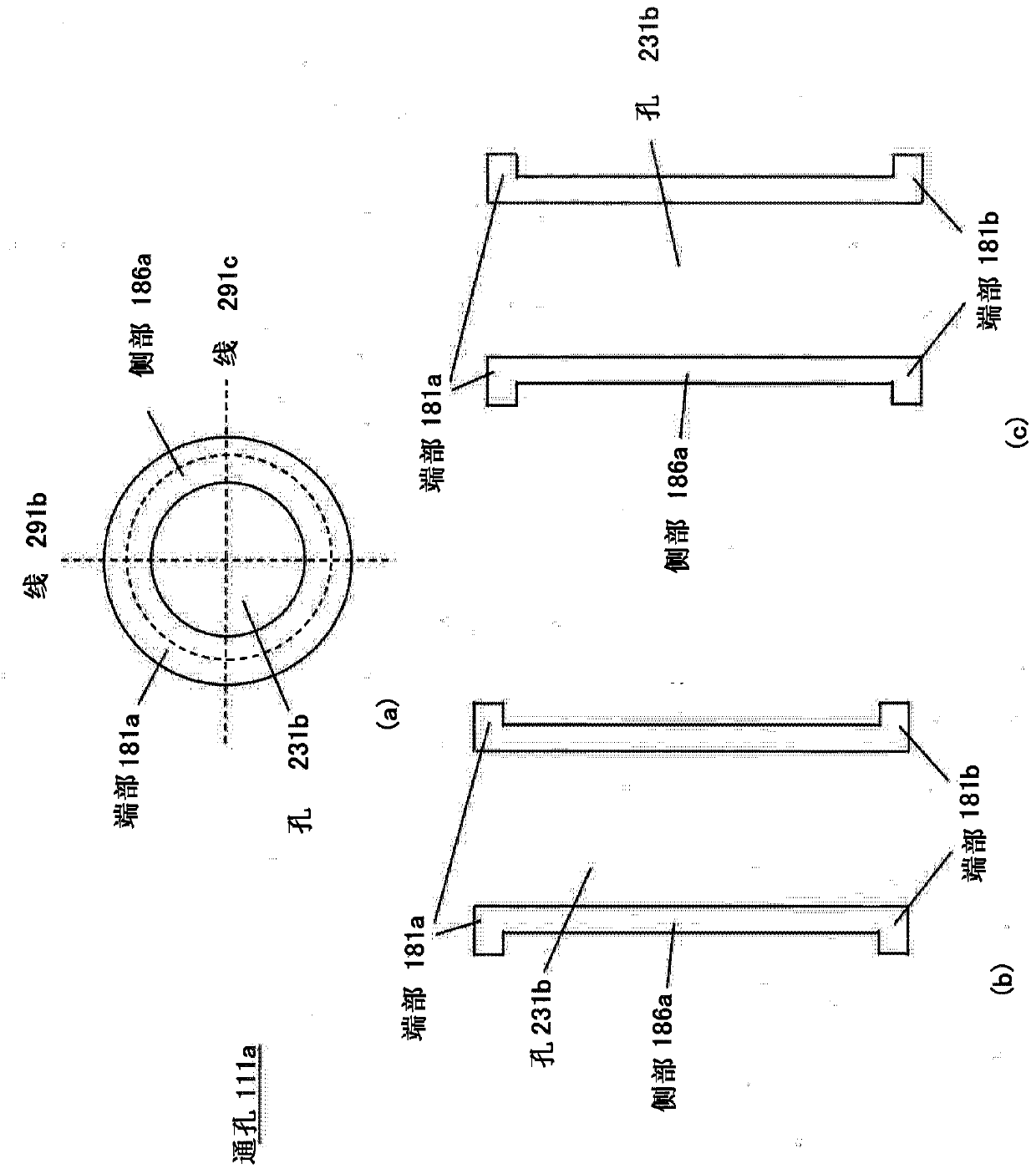
[0041] The through holes 111a and 111b are disposed in the substrate 121a in a manner of penetrating the substrate 121a. will refer to later figure 2 Details of the through holes 111a and 111b are described.

[0042] The wirings 131a and 131b are general wirings formed insi...


PUM


Abstract

The present invention addresses the problem of providing a connecting structure or similar that can minimize a decrease in a wireable region of a substrate while reducing the effect of stubs of a pairof vias on the output of a capacitor that is connected to said vias. In order to solve this problem, this connecting structure comprises: a first conductor that passes through a substrate and is provided with a first input / output section; a second conductor that passes through the substrate and is provided with a second input / output section; a first capacitor, one terminal of which being connected to a terminal of the first conductor that is on a first surface of the substrate, the other terminal of which being connected to a terminal of the second conductor that is on the first surface of the substrate; and a second capacitor or a resistor, one terminal of which being connected to a terminal of the first conductor that is on a second surface of the substrate, another terminal of which that is not connected to the one terminal being connected to a terminal of the second conductor that is on the second surface, wherein the first input / output section is provided to a portion of a side section of the first conductor, and / or the second input / output section is provided to a portion of a side section of the second conductor.

Description

technical field [0001] The present invention relates to a connection structure between a plurality of via holes. Background technique [0002] In order to bring the output of a certain circuit into an AC-coupled state with the input of another circuit, a capacitor is usually inserted between the output and the input. Here, AC is an abbreviation for Alternating Current. [0003] When such a capacitor is mounted between a pair of via holes (hereinafter, referred to as “via holes”) disposed in a substrate, the capacitor is connected between terminals of the pair of via holes exposed on one surface of the substrate. Then, the wiring incorporated in the substrate is electrically connected to a part of the side of the via hole. Therefore, there will be a stub in the via hole as a portion through which current does not flow (see Patent Documents 1 and 2). [0004] On the other hand, it has been explained that the presence of the stub leads to degradation of a predetermined outpu...

Claims


Application Information

Patent Timeline
Patent Type & Authority Applications(China)
IPC IPC(8): H05K3/46
CPCH05K2201/10015H05K2201/10545H05K2201/10636H05K1/181H05K1/114H05K3/429H05K1/0251H05K1/0239Y02P70/50H01L23/5226H01L23/5223H05K3/46H05K3/00
Inventor 上村文子柏仓和弘
Owner NEC CORP
Learn More