Lateral radiation-resistant power device structure
A power device and anti-radiation technology, which is applied in the direction of electric solid-state devices, semiconductor devices, semiconductor/solid-state device components, etc., can solve problems such as electronic equipment failure, component performance damage, etc. Irradiation, the effect of simple and feasible process difficulty
- Summary
- Abstract
- Description
- Claims
- Application Information
AI Technical Summary
Problems solved by technology
Method used
Image
Examples
Embodiment 1
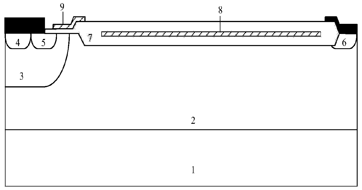
[0023] Such as figure 1 As shown, a lateral radiation-resistant power device structure includes a semiconductor substrate 1 of the second conductivity type, and a semiconductor drift region 2 of the first conductivity type located on the upper surface of the semiconductor substrate 1 of the second conductivity type is formed on the first The second conductivity type semiconductor well region 3 in the conductivity type semiconductor drift region 2, the second conductivity type semiconductor contact region 4 and the first conductivity type semiconductor contact region 5 located above the interior of the second conductivity type semiconductor well region 3 , the right side of the semiconductor contact region 4 of the second conductivity type is in contact with the semiconductor contact region 5 of the first conductivity type, and the semiconductor contact region 7 of the first conductivity type is located on the upper right side inside the drift region 2 of the semiconductor of th...
Embodiment 2
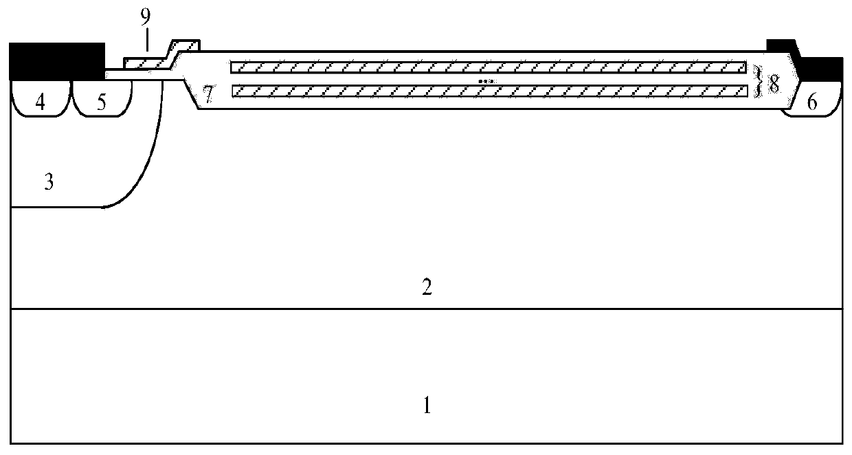
[0026] Such as figure 2 As shown, the difference between this embodiment and Embodiment 1 is that there are multiple layers of polysilicon strips 8 in the insulating layer 7 , each layer of polysilicon strips 8 are parallel to each other, and there is a longitudinal interval between adjacent polysilicon strips 8 . The vertical direction refers to the direction from the surface of the insulating layer 7 to the inside of the first conductivity type semiconductor drift region 2 .
[0027] This structure will further improve the radiation resistance of the device. There is no radiation-induced charge inside the parallel polysilicon strips. The impact of radiation on the oxide layer will be further reduced, and the modulation of the electric charge on the terminal electric field will be further reduced.
Embodiment 3
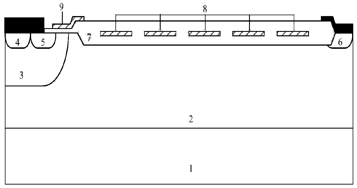
[0029] Such as image 3 As shown, the difference between this embodiment and Embodiment 1 is that the polysilicon strips 8 located in the insulating layer 7 are distributed intermittently in the lateral direction. This structure will further improve the anti-radiation capability of the terminal. A plurality of discontinuous polysilicon strips will modulate the terminal electric field in a non-radiative state and improve the withstand voltage of the device.
PUM
 Abstract
Description
Claims
Application Information


