Eureka AIR delivers breakthrough ideas for toughest innovation challenges, trusted by R&D personnel around the world.

A Lateral Radiation Hardened Power Device Structure

A power device and anti-radiation technology, which is applied in the direction of semiconductor devices, electric solid devices, semiconductor/solid device components, etc., can solve problems such as component performance damage, electronic equipment failure, etc., achieve anti-radiation reinforcement, solve anti-radiation Irradiation, the effect of simple and feasible process difficulty

Active Publication Date: 2020-12-29
UNIV OF ELECTRONICS SCI & TECH OF CHINA
View PDF8 Cites 0 Cited by
  • Summary
  • Abstract
  • Description
  • Claims
  • Application Information

AI Technical Summary

Problems solved by technology

Electronic components that make up electronic equipment are inevitably exposed to strong radiation applications such as space radiation and nuclear radiation. Radiation effects will cause damage to the performance of components to varying degrees, and cause the entire electronic equipment to fail

Method used


Image

  • A Lateral Radiation Hardened Power Device Structure
  • A Lateral Radiation Hardened Power Device Structure
  • A Lateral Radiation Hardened Power Device Structure

Examples


Embodiment 1

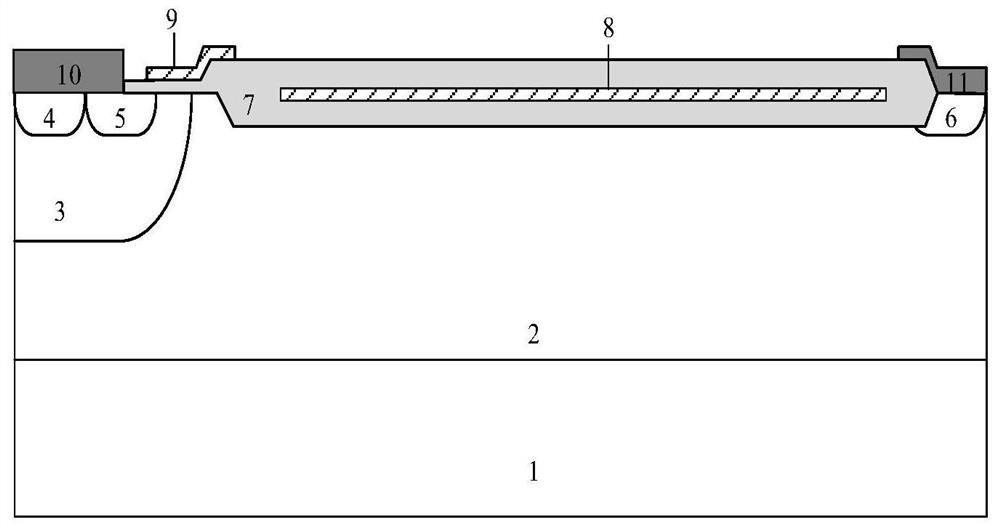
[0023] Such as figure 1 As shown, a lateral radiation-resistant power device structure includes a semiconductor substrate 1 of the second conductivity type, and a semiconductor drift region 2 of the first conductivity type located on the upper surface of the semiconductor substrate 1 of the second conductivity type is formed on the first The second conductivity type semiconductor well region 3 in the conductivity type semiconductor drift region 2, the second conductivity type semiconductor contact region 4 and the first conductivity type semiconductor contact region 5 located above the interior of the second conductivity type semiconductor well region 3 , the right side of the semiconductor contact region 4 of the second conductivity type is in contact with the semiconductor contact region 5 of the first conductivity type, and the semiconductor contact region 7 of the first conductivity type is located on the upper right side inside the drift region 2 of the semiconductor of th...

Embodiment 2

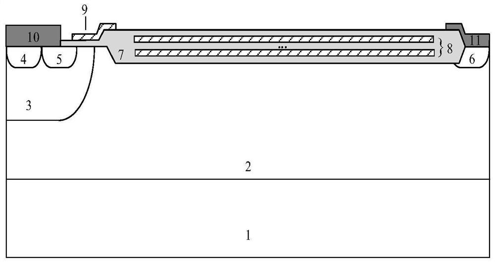
[0026] Such as figure 2 As shown, the difference between this embodiment and Embodiment 1 is that there are multiple layers of polysilicon strips 8 in the insulating layer 7 , each layer of polysilicon strips 8 are parallel to each other, and there is a longitudinal interval between adjacent polysilicon strips 8 . The vertical direction refers to the direction from the surface of the insulating layer 7 to the inside of the first conductivity type semiconductor drift region 2 .

[0027] This structure will further improve the radiation resistance of the device. There is no radiation-induced charge inside the parallel polysilicon strips. The impact of radiation on the oxide layer will be further reduced, and the modulation of the electric charge on the terminal electric field will be further reduced.

Embodiment 3

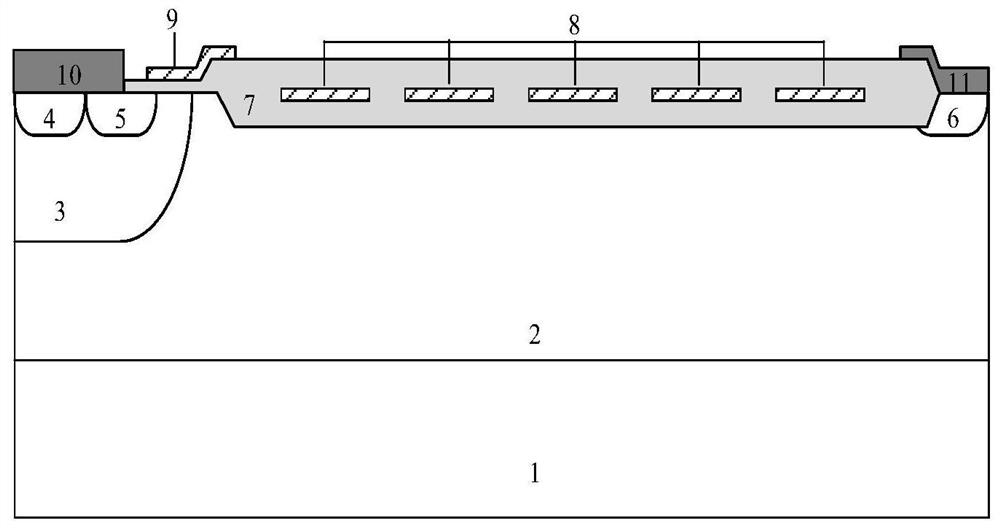
[0029] Such as image 3 As shown, the difference between this embodiment and Embodiment 1 is that the polysilicon strips 8 located in the insulating layer 7 are distributed intermittently in the lateral direction. This structure will further improve the anti-radiation capability of the terminal. A plurality of discontinuous polysilicon strips will modulate the terminal electric field in a non-radiative state and improve the withstand voltage of the device.


PUM


Abstract

The present invention provides a lateral anti-radiation power device structure, including a second conductivity type semiconductor substrate, a first conductivity type semiconductor drift region, a second conductivity type semiconductor well region, a second conductivity type semiconductor contact region, and a second conductivity type semiconductor contact region. One conductivity type semiconductor contact region, part of the upper surface of the first conductivity type semiconductor contact region and part of the upper surface of the second conductivity type semiconductor well region are covered with an insulating layer, and the left side of the first conductivity type semiconductor contact region is embedded with insulation layer; the upper left of the insulating layer is covered with polysilicon; the insulating layer is embedded with polysilicon strips, and the polysilicon layer is introduced into the thick field oxygen to prevent holes generated by radiation ionization from moving to the interface of the field oxide layer / drift region and reduce the field oxide layer. The capture rate of traps near the interface of the / drift region to holes can suppress the modulation effect of ionizing radiation trap charges on the potential field and carrier behavior in the body, and realize the radiation resistance reinforcement of devices. The invention can well solve the radiation resistance of devices according to the question.

Description

technical field [0001] The invention belongs to the technical field of power semiconductor devices, and in particular relates to a lateral anti-radiation power device structure. Background technique [0002] With the development of space technology, nuclear technology and strategic weapon technology, various electronic devices have been widely used in artificial satellites, spaceships, launch vehicles, long-range missiles and nuclear weapon control systems. Power high-voltage integratable devices represented by LDMOS devices are widely used in power high-voltage integrated circuits such as power circuits, analog switching circuits, and high-voltage drive circuits due to their characteristics of easy integration and fast switching speed. The electronic components that make up the electronic equipment are inevitably exposed to strong radiation application environments such as space radiation and nuclear radiation. Contents of the invention [0003] The object of the present...

Claims


Application Information

Patent Timeline
Patent Type & Authority Patents(China)
IPC IPC(8): H01L29/06H01L23/552
Inventor 周锌李怡袁章亦安乔明张波
Owner UNIV OF ELECTRONICS SCI & TECH OF CHINA
Why Eureka
Eureka Blog
Learn More