Flash memory and forming method thereof

A memory and flash technology, applied in the field of flash memory and its formation, can solve the problems of poor performance of split-gate flash memory, achieve high erasing efficiency, increase coupling rate, and increase coupling voltage

Active Publication Date: 2019-05-10
SHANGHAI HUAHONG GRACE SEMICON MFG CORP
View PDF6 Cites 5 Cited by
  • Summary
  • Abstract
  • Description
  • Claims
  • Application Information

AI Technical Summary

Problems solved by technology

[0004] However, the performance of existing split-gate flash memory is poor

Method used


Image

  • Flash memory and forming method thereof
  • Flash memory and forming method thereof
  • Flash memory and forming method thereof

Examples


Embodiment Construction

[0024] As mentioned in the background, the performance of the prior art flash memory is poor.

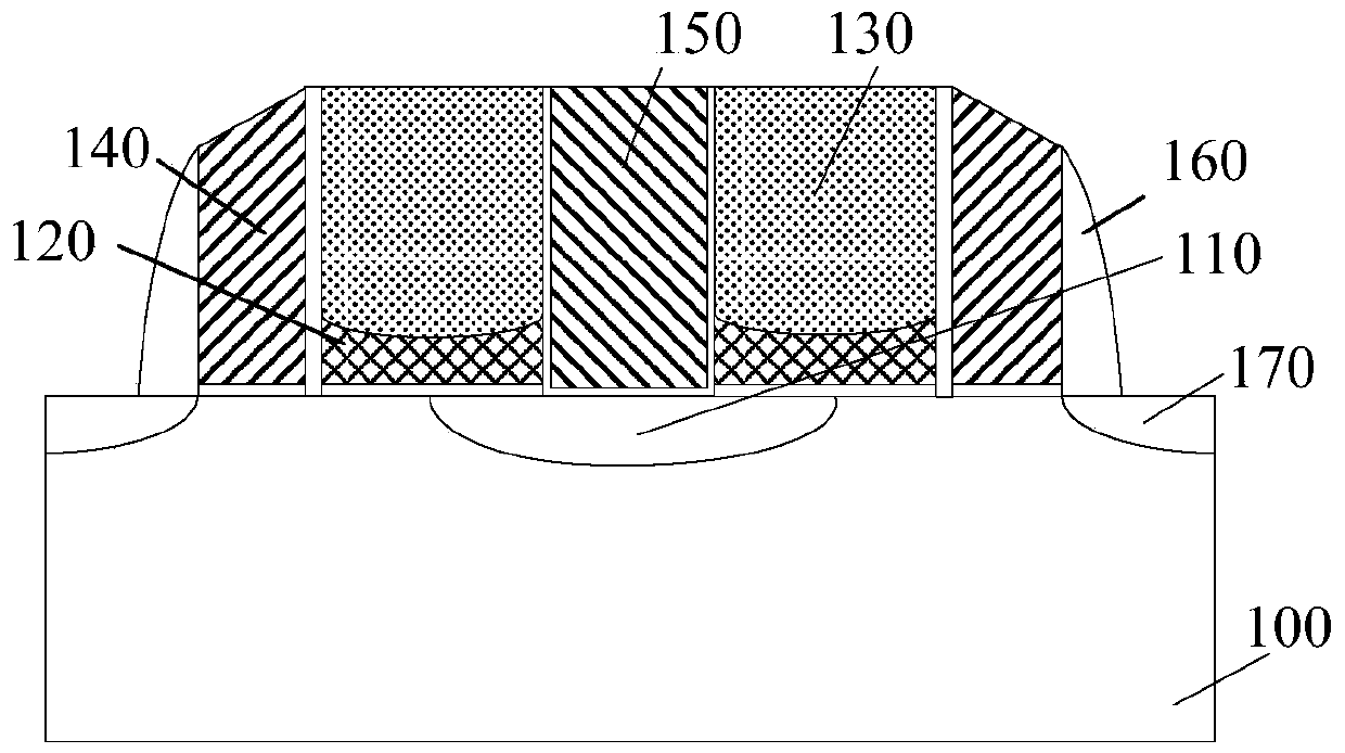
[0025] A type of flash memory, please refer to figure 1 , including: a semiconductor substrate 100, the semiconductor substrate 100 includes an erasing region and a floating gate region, the floating gate region is adjacent to the erasing region and is located on both sides of the erasing region; the erasing region located in the semiconductor substrate 100 The erasing gate structure 150 on the semiconductor substrate; the floating gate structure 120 respectively located on the floating gate region of the semiconductor substrate; the first spacer 130 located on the floating gate structure 120; covering the first spacer 130 and the floating gate The word line structure 140 of the structure side wall, the floating gate structure 120 is located between the erasing gate structure 150 and the word line structure 140; the second side wall 160 covering the side wall of the word line struct...


PUM


Abstract

The invention provides a flash memory and a forming method thereof. The flash memory comprises: a semiconductor substrate, wherein the semiconductor substrate comprises a source line region and a floating gate region, and the floating gate region is adjacent to the source line region and is located on both sides of the source line region; a source region located in the source line region of the semiconductor substrate; a source line layer located on the source region, wherein the source line layer is electrically connected with the source region; floating gate structures respectively located on the floating gate region of the semiconductor substrate, wherein the heights of the floating gate structures are greater than the height of the source line layer; and an erase gate structure locatedon the source line layer. The performance of the flash memory is improved.

Description

technical field [0001] The invention relates to the field of semiconductor manufacturing, in particular to a flash memory and a forming method thereof. Background technique [0002] Flash memory is an important device in integrated circuit products. The main feature of flash memory is that it can keep stored information for a long time without applying voltage. Flash memory has the advantages of high integration, fast access speed and easy wiring, so it is widely used. [0003] Flash memory is classified into two types: stack gate flash memory and split gate flash memory. The stacked gate flash memory has a floating gate and a control gate above the floating gate. The stacked gate flash memory has the problem of over-supply lines. Different from the stacked gate flash memory, the split gate flash memory forms a word line as a source line gate on one side of the floating gate. The split-gate flash memory can effectively avoid the over-source line effect. [0004] Howeve...

Claims


Application Information

Patent Timeline
Patent Type & Authority Applications(China)
IPC IPC(8): H01L27/11521
Inventor 于涛李冰寒
Owner SHANGHAI HUAHONG GRACE SEMICON MFG CORP
Why Eureka
Try Eureka