Method for manufacturing fast flash memory with coupling rate increased

A manufacturing method and memory technology, applied in the direction of semiconductor/solid-state device manufacturing, electrical components, circuits, etc.

Inactive Publication Date: 2003-10-01
TAIWAN SEMICON MFG CO LTD
View PDF1 Cites 4 Cited by
  • Summary
  • Abstract
  • Description
  • Claims
  • Application Information

AI Technical Summary

Problems solved by technology

Increased couplin

Method used


Image

  • Method for manufacturing fast flash memory with coupling rate increased
  • Method for manufacturing fast flash memory with coupling rate increased
  • Method for manufacturing fast flash memory with coupling rate increased

Examples


Embodiment Construction

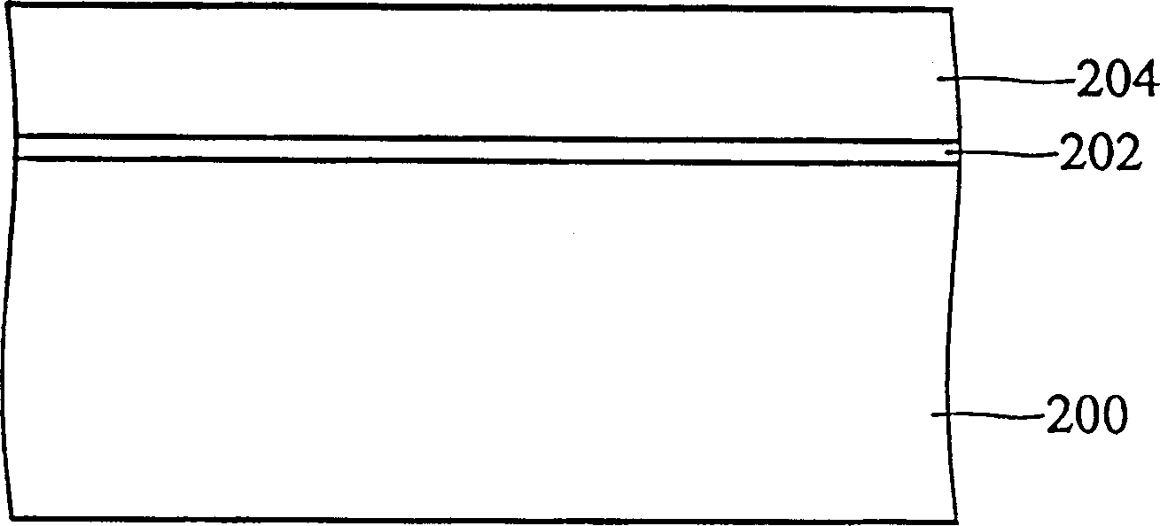
[0016] Figure 2a to Figure 2g And the manufacturing method of the flash memory with increased coupling ratio according to the first embodiment of the present invention is described. First, please refer to Figure 2a , provide a semiconductor substrate 200, such as a silicon wafer, on the substrate 200, deposit and form an insulating layer 202, such as an oxide layer, and a hard mask layer (hardmask) 204, such as a silicon nitride layer, with a thickness of about 110 Angstroms () and 1600.

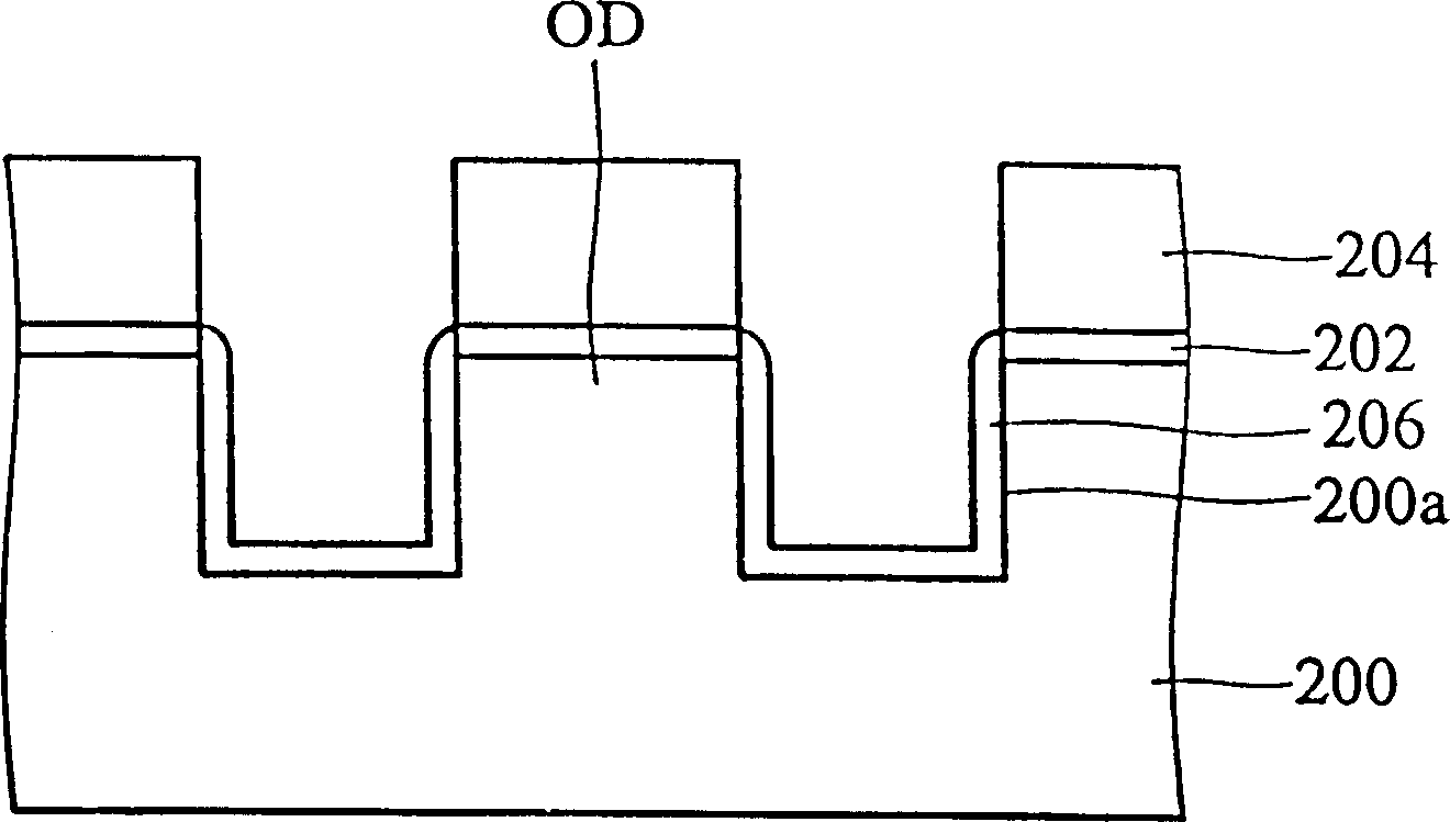
[0017] Next, please refer to Figure 2b , in order to define the active region OD, first define and etch the hard mask layer 204 to expose the insulating layer 202, and then use the patterned hard mask layer 204 as a mask to etch the exposed oxide layer 202 and the semiconductor substrate 200 surface below. The semiconductor substrate 200 is formed with two trenches 200a as isolation structures. Then, a pad oxide layer 206 with a thickness of about 200 Å is formed on the inner wall o...


PUM


Abstract

The prewent invention discloses a manufacture method for flash memory to increasethe coupling ratio, which first defines two isolation structures projected above the surface of semiconductor substrate and then executes ion implanting so as to form adoping region on the semiconductor substrate at two sides of the isolation structure as well as forms dielectric isolation part at the side wall of two projected isolation structures, and at least, forms tunnelling dielectric layer and floating grid between the dielectric isolation parts in sequence to make the lower surface area of the floating grid smaller than the upper surface area of it for increasing the capacity coupling ratio.

Description

technical field [0001] The invention relates to a manufacturing method of a storage element, especially a manufacturing method of a flash memory, which has a high coupling rate and increases the efficiency of programming and erasing. Background technique [0002] With the development of semiconductor process technology, flash memory with faster access speed has been developed in storage devices, which has separate gates of control gate and floating gate, and in order to save circuit layout space , Usually every two bits share a source / drain for writing, reading and erasing operations. On the other hand, in the production of flash memory nowadays, the isolation technology of shallow trench isolation (STI) is used to replace the traditional local oxidation of silicon (LOCOS) to isolate the active area (OD). In order to realize the purpose of reducing the size of the storage device, and then effectively improve the integration degree of the semiconductor device. [0003] fig...

Claims


Application Information

Patent Timeline
IPC IPC(8): H01L21/8239H01L21/8246
Inventor 谢佳达
Owner TAIWAN SEMICON MFG CO LTD
Why Eureka
Try Eureka