Cell recess oxide etching method of improving deep-submicron flash memory device coupling rate

A flash memory device, deep submicron technology, applied in the direction of electric solid device, semiconductor device, semiconductor/solid device manufacturing, etc., to achieve the effect of overcoming uneven density

Active Publication Date: 2016-08-03
SHANGHAI HUALI MICROELECTRONICS CORP
View PDF3 Cites 5 Cited by
  • Summary
  • Abstract
  • Description
  • Claims
  • Application Information

AI Technical Summary

Problems solved by technology

[0018] The technical problem to be solved by the present invention is to reduce the difference in height of the bottom of the oxide in the trench, unify the oxide sidewall of the polycrystalline floating gate, and uniform the contact area bet

Method used


Image

  • Cell recess oxide etching method of improving deep-submicron flash memory device coupling rate
  • Cell recess oxide etching method of improving deep-submicron flash memory device coupling rate
  • Cell recess oxide etching method of improving deep-submicron flash memory device coupling rate

Examples


Embodiment Construction

[0041] In order to make the content of the present invention clearer and easier to understand, the content of the present invention will be further described below in conjunction with the accompanying drawings. Of course, the present invention is not limited to this specific embodiment, and general replacements known to those skilled in the art are also covered within the protection scope of the present invention.

[0042] Secondly, the present invention is described in detail by means of schematic diagrams. When describing the examples of the present invention in detail, for the convenience of explanation, the schematic diagrams are not partially enlarged according to the general scale, which should not be used as a limitation of the present invention.

[0043] Embodiments of the present invention will be further described below in conjunction with the accompanying drawings.

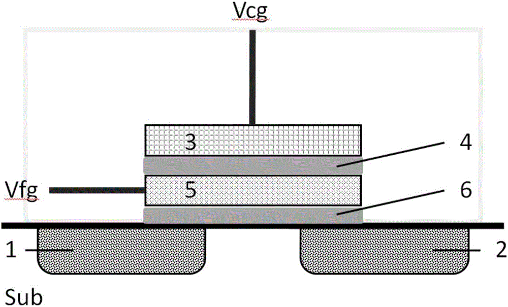
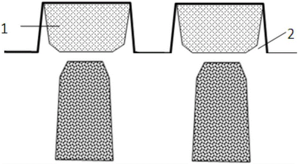
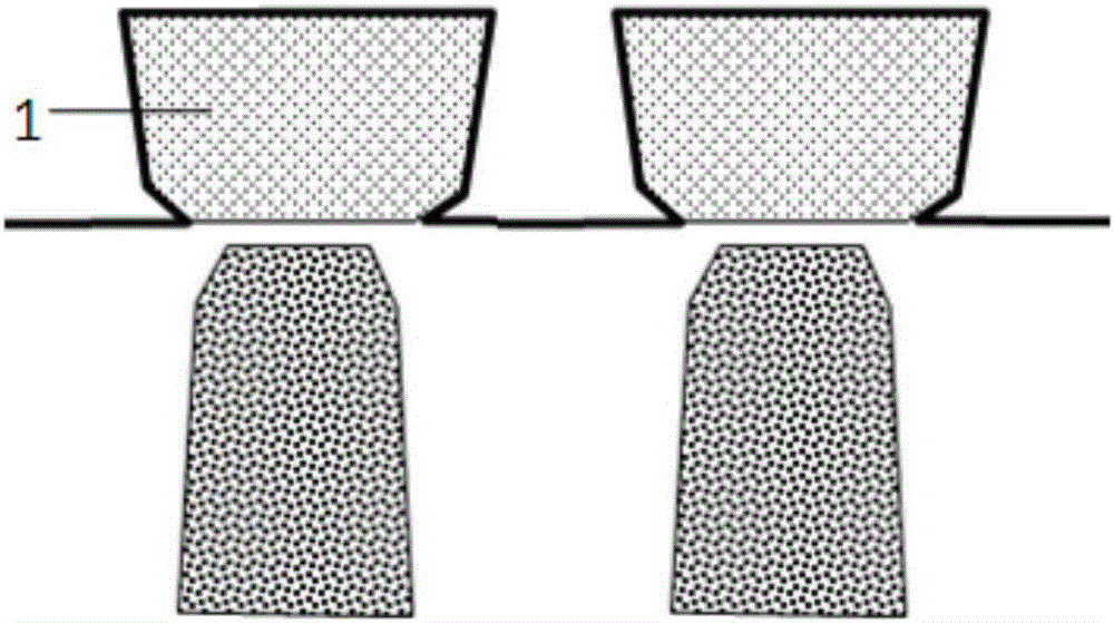
[0044] In this embodiment, a deep submicron level self-aligned polycrystalline flash memory process ...


PUM


Abstract

The present invention provides a cell recess oxide etching method of improving a deep-submicron flash memory device coupling rate. The method is characterized by combining a first dry etching step, a wet etching step and a second dry etching step; the dry etching effectively overcomes the characteristic that the density of the filling oxides is uneven, and the oxides in a density loose area at an opening in a cell recess are removed by the first dry etching step, so that the subsequently etched oxide interfaces are same in height and even and consistent in density; then, the oxide side walls at the side walls of the polycrystalline floating gates caused by the first dry etching are removed by the wet etching, so that the side walls are totally not covered by the oxides; and then, the cell recess oxide bottoms of consistent height and the oxide side walls at the bottoms of the side walls of the polycrystalline floating gates of uniform morphology and protecting the tunneling oxide layers are realized by the second dry etching, and then the ONO deposition is carried out to form the consistent ONO capacitors formed by the contact of the ONO and the polycrystalline floating gates, thereby achieving the purposes of improving the coupling rate of a deep-submicron flash memory device and improving the product qualified rate and service life.

Description

technical field [0001] The invention relates to the technical field of integrated circuit manufacturing, in particular to a trench oxide etching method for improving the coupling rate of deep submicron flash memory devices. Background technique [0002] With the continuous development of integrated circuit manufacturing process, the feature size of devices is also continuously reduced. The technology of submicron and deep submicron flash memory devices is becoming more and more mature. As an important structure for storing data in flash memory devices, polycrystalline floating gate transistors have been improved by the market. requirements are quite urgent. [0003] figure 1 It is the basic structure of a polycrystalline floating gate transistor as a basic storage unit (cell). [0004] As shown in the figure, each polycrystalline floating gate transistor is a three-terminal device, which are source 1, drain 2 and gate 3 respectively. The effect of the electric field is us...

Claims


Application Information

Patent Timeline
IPC IPC(8): H01L27/115H01L21/311H01L21/28H01L21/8247
CPCH01L29/40114H01L21/31111H01L21/31116H10B41/30
Inventor 黄海辉杨渝书乔夫龙李程
Owner SHANGHAI HUALI MICROELECTRONICS CORP
Why Eureka
Try Eureka