

Thin film transistor and its manufacturing method, device, chip and display device
A thin-film transistor and basic technology, applied in the manufacture of transistors, semiconductor devices, semiconductor/solid-state devices, etc., can solve the problems of large source and drain spacing, large size of thin film transistors, and low precision, and achieve the effect of reducing size
- Summary
- Abstract
- Description
- Claims
- Application Information
AI Technical Summary
Problems solved by technology
Method used
Image

Examples
Embodiment Construction
[0052] In order to make the purpose, technical solution and advantages of the present application clearer, the implementation manners of the present application will be further described in detail below in conjunction with the accompanying drawings.
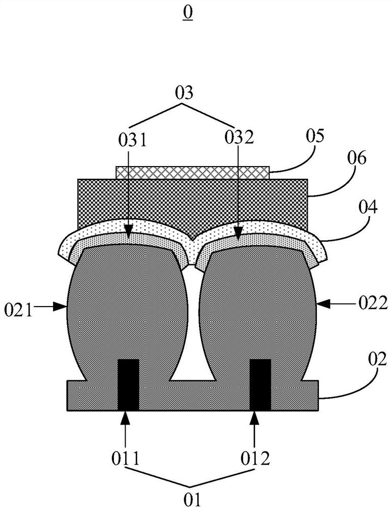
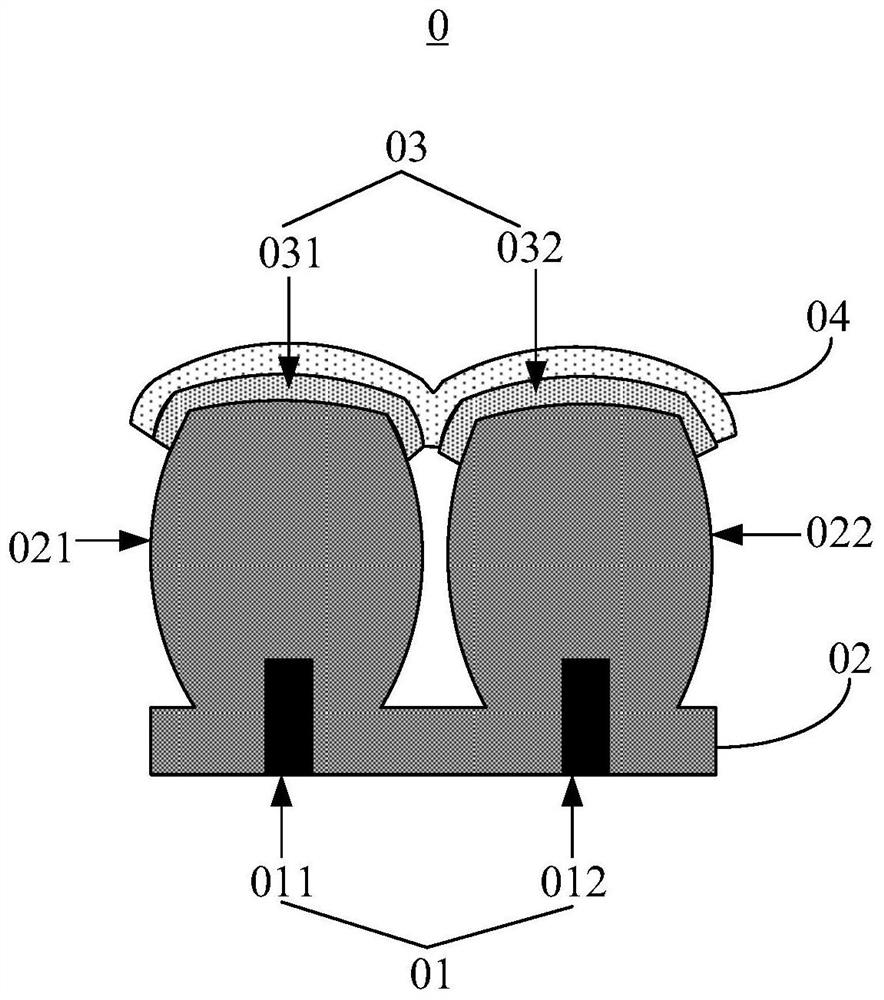
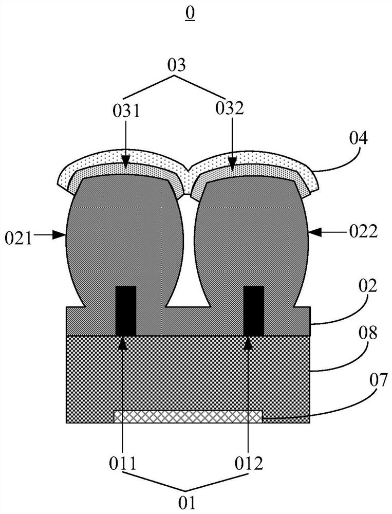
[0053] Due to the low precision of the patterning process in the related art, the distance between the source and the drain is often large, resulting in a large size of the thin film transistor. Therefore, an embodiment of the present invention provides a thin film transistor, and the thin film transistor The source and drain layers can be manufactured by deposition. Due to the high precision of layer formation in the way of deposition, the distance between the source and the drain can be reduced, and the size of the thin film transistor can be reduced. The thin film transistor and its manufacturing method provided by the embodiments of the present invention will be explained below.
[0054] Exemplarily, figure 1 A schematic st...
PUM
| Property | Measurement | Unit |
|---|---|---|
| depth | aaaaa | aaaaa |
| depth | aaaaa | aaaaa |
| width | aaaaa | aaaaa |
Abstract
Description
Claims
Application Information