Optical fingerprint sensor structure and electronic device

A fingerprint sensor and electronic equipment technology, applied in chemical instruments and methods, instruments, coatings, etc., can solve problems such as print marks on photosensitive films, and achieve the effect of improving accuracy and beautiful structure of optical fingerprint sensors

Pending Publication Date: 2019-05-14
LENS TECH CHANGSHA
View PDF0 Cites 0 Cited by
  • Summary
  • Abstract
  • Description
  • Claims
  • Application Information

AI Technical Summary

Problems solved by technology

[0005] In view of this, the purpose of the embodiments of the present invention is to provide an optical fingerprint sensor structure to improve the problem of imprints after the photosensitive film is bonded

Method used


Image

  • Optical fingerprint sensor structure and electronic device
  • Optical fingerprint sensor structure and electronic device
  • Optical fingerprint sensor structure and electronic device

Examples


no. 1 example

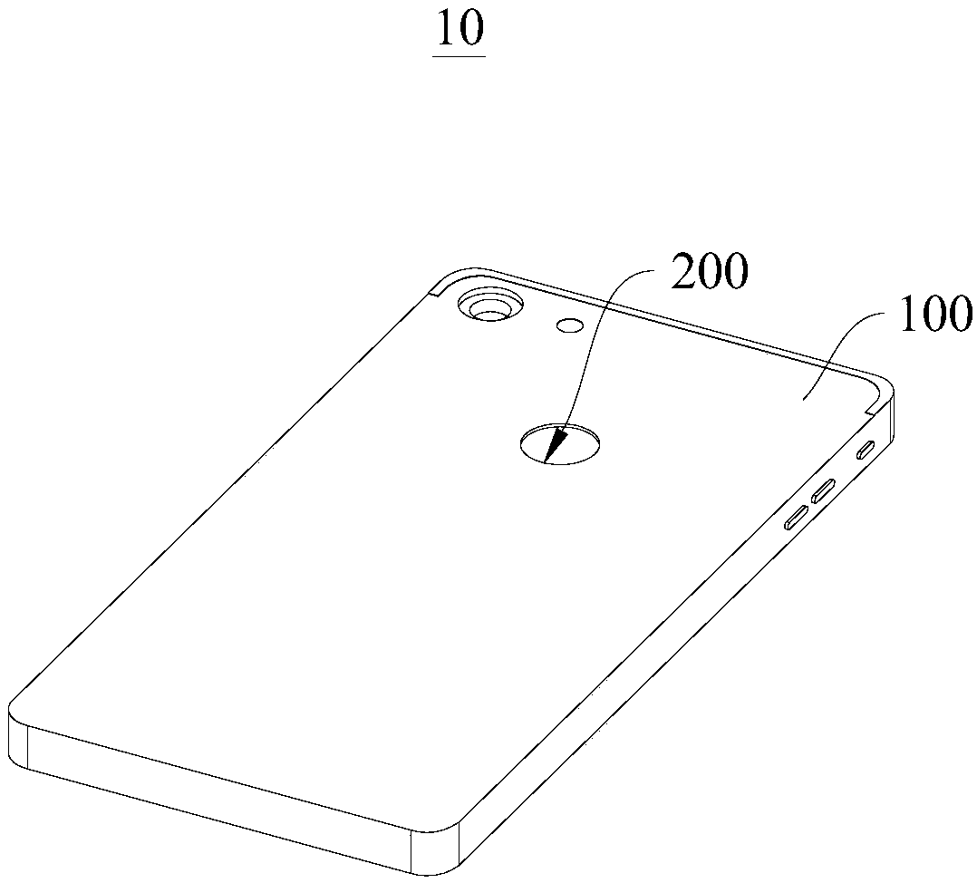
[0034] see figure 1 , this embodiment provides an electronic device 10 , the electronic device 10 includes an electronic device body 100 and an optical fingerprint sensor structure 200 , and the optical fingerprint sensor structure 200 is disposed on the electronic device body 100 .

[0035] The electronic device 10 can be any device that can support the optical fingerprint sensor structure 200. For example, the electronic device 10 can be a mobile phone, a tablet computer, a notebook computer or other electronic devices 10. In this embodiment, the electronic device 10 can be a mobile phone, but is not limited to this.

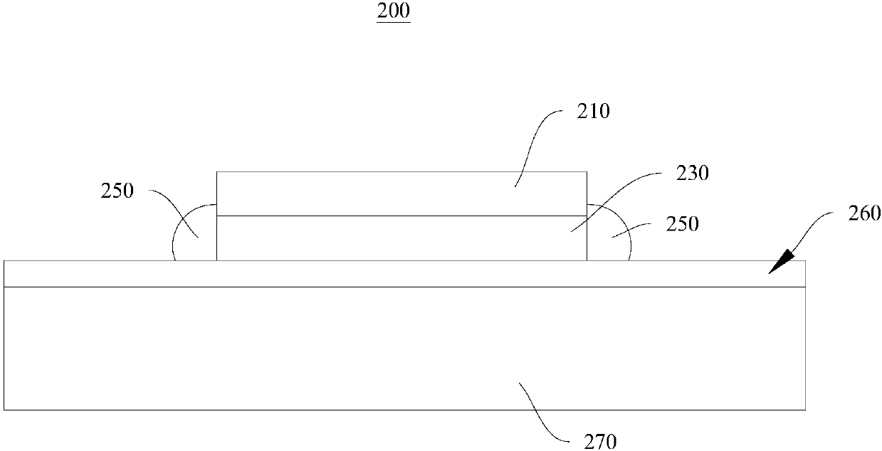
[0036] The optical fingerprint sensor structure 200 includes an optical fingerprint sensor 210 , a first adhesive layer 230 , a structural adhesive 250 , a photosensitive film 260 and a substrate 270 . see figure 2 , figure 2 A schematic structural diagram of the optical fingerprint sensor structure 200 provided by the present invention is shown.

[0037...

no. 2 example

[0052] This embodiment provides an optical fingerprint sensor structure 200. It should be noted that the basic principle of the optical fingerprint sensor structure 200 provided in this embodiment is basically the same as that of the optical fingerprint sensor structure 200 provided in the first embodiment. For a brief description, Please refer to the first embodiment for the parts not mentioned in this embodiment.

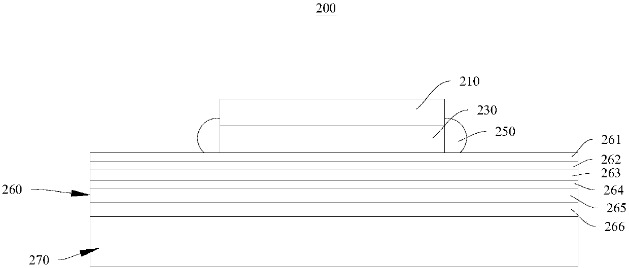
[0053] In the optical fingerprint sensor structure 200 provided in this embodiment, the thickness of the cover ink layer 261 is greater than 16 microns due to process requirements (such as printing LOGO or patterns), for example, it can be 20 microns; the thickness of the color ink layer 262 Thickness greater than 25 microns.

[0054] Both the cover ink layer 261 and the color ink layer 262 are added with a hardener, such as isocyanate, to increase the hardness of the cover ink layer 261 and the color ink layer 262, and prevent the excessive internal stress of the...


PUM

PropertyMeasurementUnit
thicknessaaaaaaaaaa
thicknessaaaaaaaaaa
thicknessaaaaaaaaaa

Abstract

The invention provides an optical fingerprint sensor structure and an electronic device, and relates to the technical field of fingerprint sensors. The optical fingerprint sensor structure comprises an optical fingerprint sensor, a first adhesive layer, a photosensitive film and a substrate. The photosensitive film comprises a thin film layer and a second glue layer, the optical fingerprint sensoris bonded with the thin film layer through the first glue layer, the photosensitive film is bonded with the substrate through the second glue layer, the thickness of the thin film layer is smaller than 10 micrometers, and the thickness of the second glue layer is not larger than 25 micrometers. By reasonably controlling the thicknesses of the second glue layer and the thin film layer, the problemthat the attaching area contracts after the optical fingerprint sensor is attached and cured can be effectively solved, so that the attaching area cannot generate impressions, the impressions cannotbe observed from one side of the substrate, and on one hand, the accuracy of the optical fingerprint sensor is improved; And on the other hand, the optical fingerprint sensor is more attractive in structure and appearance.

Description

technical field [0001] The invention relates to the technical field of fingerprint sensors, in particular to an optical fingerprint sensor structure and electronic equipment. Background technique [0002] The fingerprint sensor is the key device to realize the automatic collection of fingerprints. According to the sensing principle, that is, the principle and technology of fingerprint imaging, the fingerprint sensor can be divided into optical fingerprint sensor, semiconductor capacitive sensor, semiconductor thermal sensor, semiconductor pressure sensor, ultrasonic sensor and radio frequency sensor. RF sensors, etc. The manufacturing technology of fingerprint sensor is a high-tech with strong comprehensiveness, high technical complexity and difficult manufacturing process. [0003] Among them, the optical fingerprint sensor mainly uses the principle of refraction and reflection of light. The light shoots from the bottom to the prism and exits through the prism. will be di...

Claims


Application Information

Patent Timeline
Patent Type & Authority Applications(China)
IPC IPC(8): G06K9/00G06K9/20B05D7/24B32B33/00B32B27/36B32B17/00B32B17/10B32B27/06B32B15/00B32B15/09
Inventor 周群飞
Owner LENS TECH CHANGSHA
Why Eureka
Try Eureka