Vertical-structure LED chip and fabrication method thereof

A LED chip and vertical structure technology, applied in the direction of electrical components, circuits, semiconductor devices, etc., can solve the problems of increased manufacturing cost of photolithography process, achieve the effect of shortening the manufacturing cycle, reducing manufacturing cost, and simplifying the manufacturing process

Active Publication Date: 2019-05-17
晶能光電股份有限公司
View PDF13 Cites 2 Cited by
  • Summary
  • Abstract
  • Description
  • Claims
  • Application Information

AI Technical Summary

Benefits of technology

The technical effect of this patented technology relates to an improved design for making semiconductor devices that have better performance at higher temperatures than previous designs while also being easier to produce without requiring multiple steps like lamination or etching techniques. This innovative technique simplifies production costs and reduces overall product size compared to existing methods. Additionally, it provides enhanced protection against damage from external factors such as water vapor during use due to its unique arrangement between layers.

Problems solved by technology

This patented technical problem addressed in this patents relates to how to create a more efficient way for producing verticality type LED chains with improved brightness levels while reducing costs associated therewith. Current methods require multiple steps involving different materials that are difficult to control accurately during production processes due to their unique properties.

Method used


Image

  • Vertical-structure LED chip and fabrication method thereof
  • Vertical-structure LED chip and fabrication method thereof
  • Vertical-structure LED chip and fabrication method thereof

Examples


Embodiment Construction

[0043] In order to more clearly illustrate the embodiments of the present invention or the technical solutions in the prior art, the specific implementation manners of the present invention will be described below with reference to the accompanying drawings. Obviously, the accompanying drawings in the following description are only some embodiments of the present invention, and those skilled in the art can obtain other accompanying drawings based on these drawings and obtain other implementations.

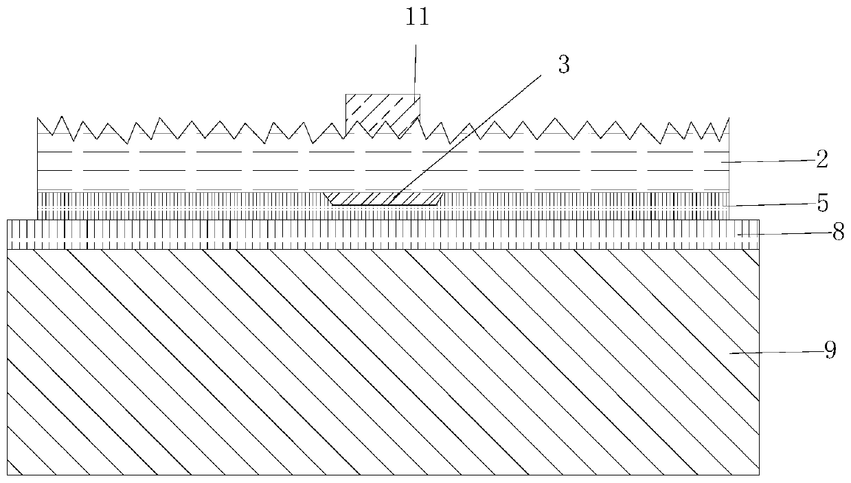
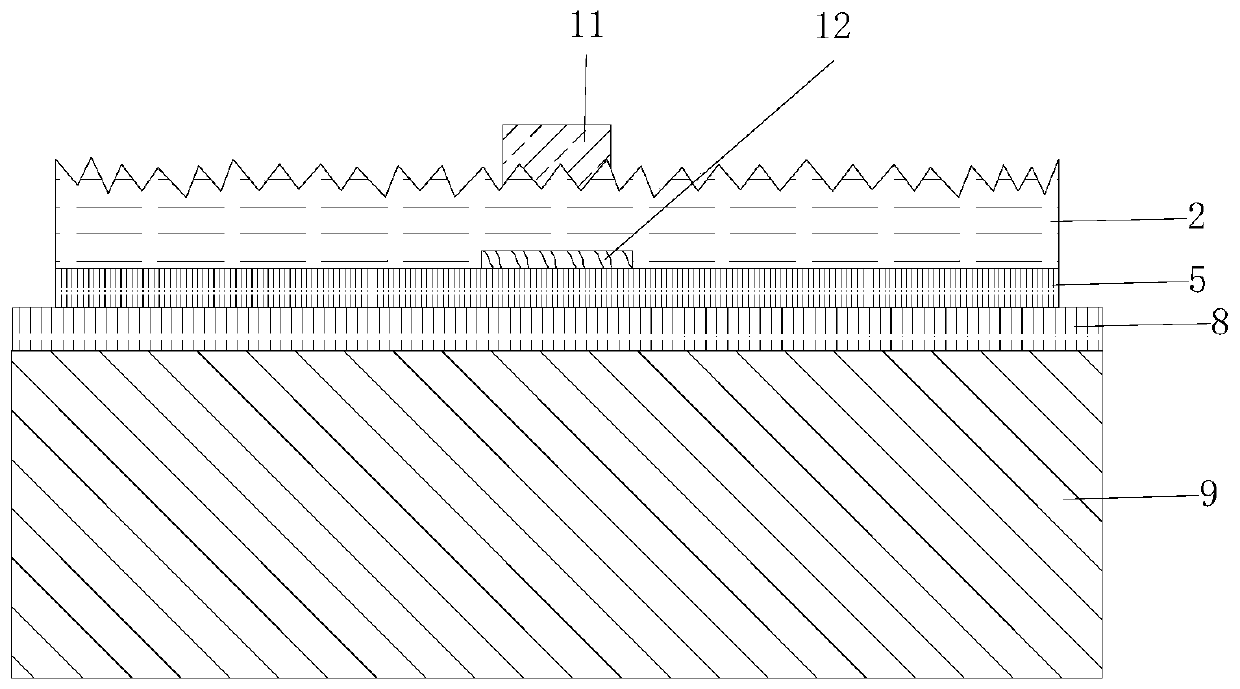
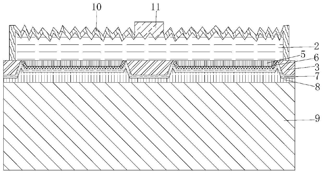
[0044] Such as image 3 Shown is a schematic structural diagram of the vertical structure LED chip provided by the present invention. As shown in the figure, the vertical structure LED chip includes: a supporting substrate; a bonding metal layer disposed on the surface of the supporting substrate; a bonding metal layer disposed on the surface of the bonding metal layer The reflective metal layer; the barrier layer area used to prepare the current barrier layer and the electrode ar...


PUM


Abstract

The invention provides a vertical-structure LED chip and a fabrication method thereof. The LED chip comprises a support substrate, a bonding alloy metal layer, a reflection metal layer, a blocking layer region, an electrode region, an epitaxial structure, an n electrode and a passivation layer, wherein the bonding alloy metal layer is arranged on a surface of the support substrate, the reflectionmetal layer is arranged on a surface of the bonding alloy metal layer, the blocking layer region is arranged on a surface of the reflection metal layer and is used for fabricating a current blocking layer, the electrode region is used for fabricating a p electrode, the epitaxial structure is arranged on surfaces of the blocking region and the electrode region, the n electrode is arranged on a surface of the epitaxial structure and is arranged opposite to the blocking layer region in a vertical direction, a boundary of the n electrode does not exceed a boundary of the blocking region, the passivation layer is arranged on a surface, except the n electrode region and a side wall, of the epitaxial structure. The LED chip is simple in fabrication process and high in light giving-out efficiency.

Description


Claims


Application Information

Patent Timeline
Owner 晶能光電股份有限公司
Why Eureka
Try Eureka