Supercharge Your Innovation With Domain-Expert AI Agents!

Controlling a semiconductor switch in a switched mode

A semiconductor, running technology, applied in the field of semiconductor switches that are controlled during on-off operation, can solve the problems of semiconductor switch pulse excitation energy converter performance damage, etc., and achieve the effect of reducing shortcomings

Pending Publication Date: 2019-05-21
VALEO EAUTOMOTIVE GERMANY GMBH
View PDF9 Cites 0 Cited by
  • Summary
  • Abstract
  • Description
  • Claims
  • Application Information

AI Technical Summary

Problems solved by technology

The performance of the semiconductor switch and of the pulsed energy converter comprising the semiconductor switch is thereby compromised

Method used


Image

  • Controlling a semiconductor switch in a switched mode
  • Controlling a semiconductor switch in a switched mode
  • Controlling a semiconductor switch in a switched mode

Examples


Embodiment Construction

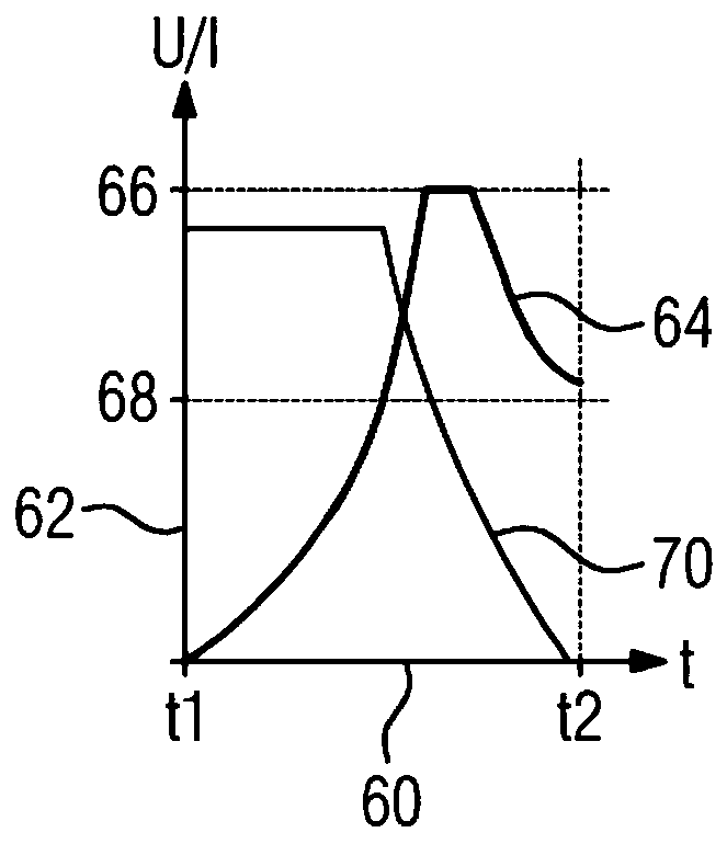
[0043] figure 1 In the schematic illustration, a graph is shown with which the switching behavior of the insulated-gate bipolar transistor 10 is shown taking active clamping into account. exist figure 1 The abscissa 60 in the graph represents the time axis, otherwise, in figure 1 The ordinate 62 of the graph in , shows not only the current through the contact gap 12 of the IGBT 10 but also the contact gap voltage of the contact gap of the IGBT 10 . The current is shown with graph 70 , whereas the corresponding voltage is shown with graph 64 . In addition, in figure 1 A line is shown in , which has the reference numeral 66 and which shows the maximum voltage of the active clamping function. Use 68 to express in figure 1 The straight line in the diagram of , which shows the supply voltage for the insulated-gate bipolar transistor 10 , is currently the intermediate circuit voltage of the DC intermediate circuit not shown further.

[0044] Depend on figure 1 It can be seen ...


PUM


Abstract

The invention relates to a method for controlling a semiconductor switch (10) in a switched mode, in which a switching path (12) of the semiconductor switch (10) is controlled by means of an electrical switching potential at a control electrode (14) of the semiconductor switch (10) in such a manner that the switching path (12) assumes a switched-off or a switched-on state according to the electrical switching potential. During a switching process of the switching path (12) from the switched-on state to the switched-off state, an electrical switching path voltage at the switching path (12) is measured and, if the switching path voltage reaches a maximum voltage, an electrical limiting potential which puts the switching path (12) into an electrically conductive state is applied to the control electrode (14) to limit the switching path voltage to the maximum voltage. A temperature of the switching path (12) is measured by means of a temperature sensor (96) coupled thermally to the switching path (12), and the maximum voltage is determined according to the measured temperature.

Description

technical field [0001] The invention relates to a method for controlling a semiconductor switch in switching operation, in which method the contact gap of the semiconductor switch is controlled by means of an electrical switching potential at the control electrode of the semiconductor switch such that The contact gap assumes the OFF or ON state depending on the electrical ON potential, wherein during the switching process of the contact gap from the ON state to the OFF state, the electrical contact gap voltage at the contact gap is detected and the maximum When the voltage is applied, the control electrode is subjected to an electrical limiting potential via the contact gap voltage, which limits the contact gap to a conductive state in order to limit the contact gap voltage to a maximum voltage. Furthermore, the invention relates to a control circuit for controlling a semiconductor switch in switch-on operation, wherein the semiconductor switch has a contact gap controllable v...

Claims


Application Information

Patent Timeline
Patent Type & Authority Applications(China)
IPC IPC(8): H03K17/082H03K17/14
CPCH03K17/0828H03K17/14
Inventor 霍格尔·霍夫曼丹尼尔·齐茨曼
Owner VALEO EAUTOMOTIVE GERMANY GMBH
Features
  • R&D
  • Intellectual Property
  • Life Sciences
  • Materials
  • Tech Scout
  • Unparalleled Data Quality
  • Higher Quality Content
  • 60% Fewer Hallucinations
Learn More