
Memory circuit, self-adaptive negative voltage write auxiliary control method and chip

A memory circuit and self-adaptive control technology, applied in the field of memory, can solve problems such as writing difficulties, achieve balance, increase success probability, and guarantee success rate

Active Publication Date: 2019-05-24
CHENGDU HAIGUANG INTEGRATED CIRCUIT DESIGN CO LTD
View PDF8 Cites 0 Cited by
  • Summary
  • Abstract
  • Description
  • Claims
  • Application Information

AI Technical Summary

Problems solved by technology

[0003] Due to process fluctuations (such as process deviations), power supply voltage drops, etc., the storage cells of the memory often have writing difficulties. Therefore, how to improve the write success rate of the memory has always been a problem considered by those skilled in the art.

Method used


Image

  • Memory circuit, self-adaptive negative voltage write auxiliary control method and chip
  • Memory circuit, self-adaptive negative voltage write auxiliary control method and chip
  • Memory circuit, self-adaptive negative voltage write auxiliary control method and chip

Examples


Embodiment Construction

[0031] The following will clearly and completely describe the technical solutions in the embodiments of the present invention with reference to the accompanying drawings in the embodiments of the present invention. Obviously, the described embodiments are only some, not all, embodiments of the present invention. Based on the embodiments of the present invention, all other embodiments obtained by persons of ordinary skill in the art without making creative efforts belong to the protection scope of the present invention.

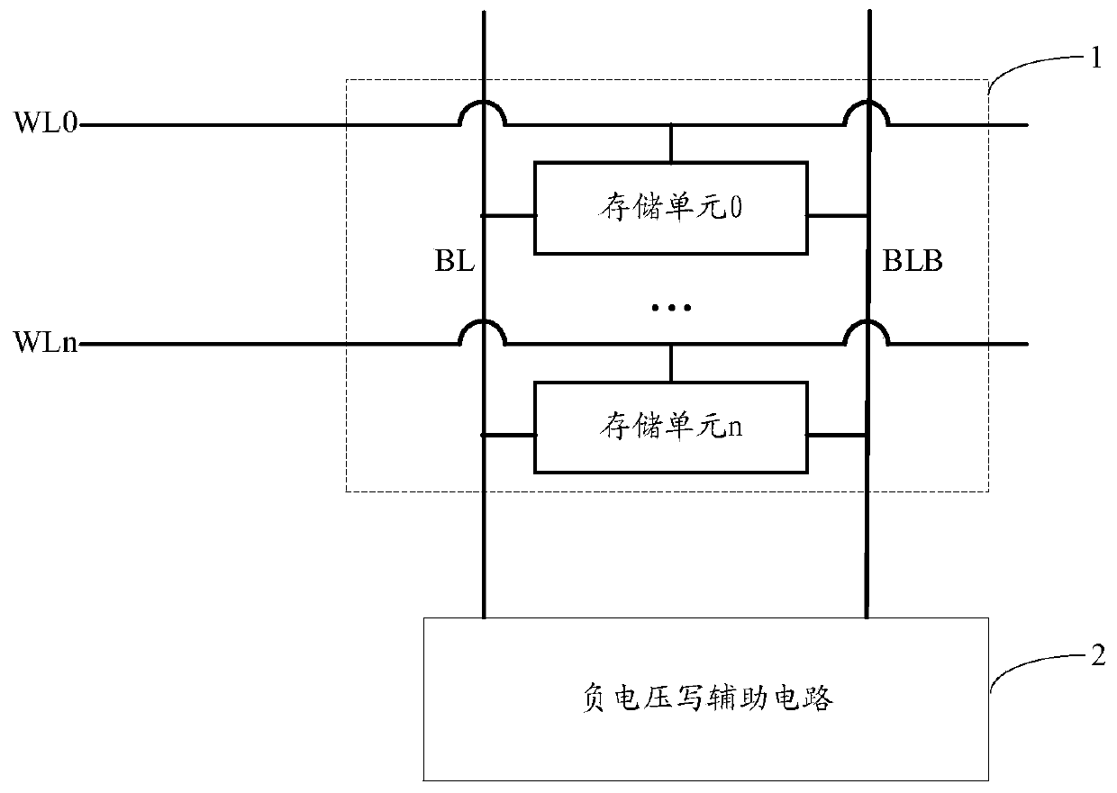
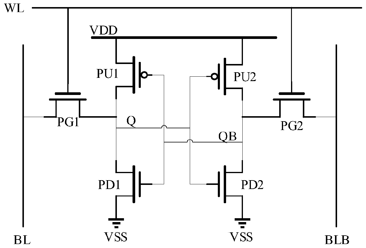
[0032] optional, figure 1 shows an alternative structure of the memory circuit, as figure 1 The shown memory circuit may include: a memory array 1 and a negative voltage write auxiliary circuit 2 .

[0033] Wherein, the storage array 1 may be an array structure composed of a plurality of storage units, and the storage unit is a basic unit structure for storing data; optionally, refer to figure 1 , the storage array can consist of:

[0034] multiple storage ...


PUM


Abstract

The invention provides a memory circuit, a self-adaptive negative voltage write auxiliary control method and a chip. The memory circuit comprises a memory array; The negative voltage write auxiliary circuit is connected with the storage array and used for adjusting the working state of the negative voltage applied to the bit line pair according to the state of the negative voltage write enable signal; The negative voltage write enable signal self-adaptive control circuit is connected with the negative voltage write assist circuit and transmits a negative voltage write enable signal to the negative voltage write assist circuit; The negative voltage write enable signal self-adaptive control circuit comprises a copy storage array which is a copy structure of the storage array; And the negative voltage write auxiliary circuit is used for detecting the data writing condition of the copy storage array, and adjusting the state of the negative voltage write enable signal according to the detected data writing condition, so as to control the negative voltage write auxiliary circuit to adjust the working state of the negative voltage through the negative voltage write enable signals in different states. The write success rate of the memory can be improved, and the power consumption cost of the memory is reduced.

Description

technical field [0001] Embodiments of the present invention relate to the technical field of memory, and in particular to a memory circuit, an adaptive negative voltage write assist control method, and a chip. Background technique [0002] Memory is a device used to store data in a chip. As a typical memory, static memory is widely used in scenarios that require high-speed data storage due to its advantages of low power consumption and fast reading speed (for example, static memory can be used for data processing system and store data), a typical static memory such as SRAM (Static Random-Access Memory, static random access memory) and the like. [0003] Due to process fluctuations (such as manufacturing process deviations), power supply voltage drop, etc., the storage cells of the memory are often difficult to write. Therefore, how to improve the write success rate of the memory has always been a problem considered by those skilled in the art. Contents of the invention ...

Claims


Application Information

Patent Timeline
IPC IPC(8): G11C11/419G11C11/412
Inventor 姚其爽
Owner CHENGDU HAIGUANG INTEGRATED CIRCUIT DESIGN CO LTD
Learn More