Organic light emitting display panel and manufacturing method thereof
A technology of light-emitting display and manufacturing method, which is applied in semiconductor/solid-state device manufacturing, semiconductor devices, electrical components, etc., and can solve problems such as affecting the effect of water and oxygen isolation.
- Summary
- Abstract
- Description
- Claims
- Application Information
AI Technical Summary
Problems solved by technology
Method used
Image

Examples
Embodiment Construction
[0026] The present invention will be further described in detail below in conjunction with the accompanying drawings and embodiments. It should be understood that the specific embodiments described here are only used to explain the present invention, but not to limit the present invention. In addition, it should be noted that, for the convenience of description, only some structures related to the present invention are shown in the drawings but not all structures.
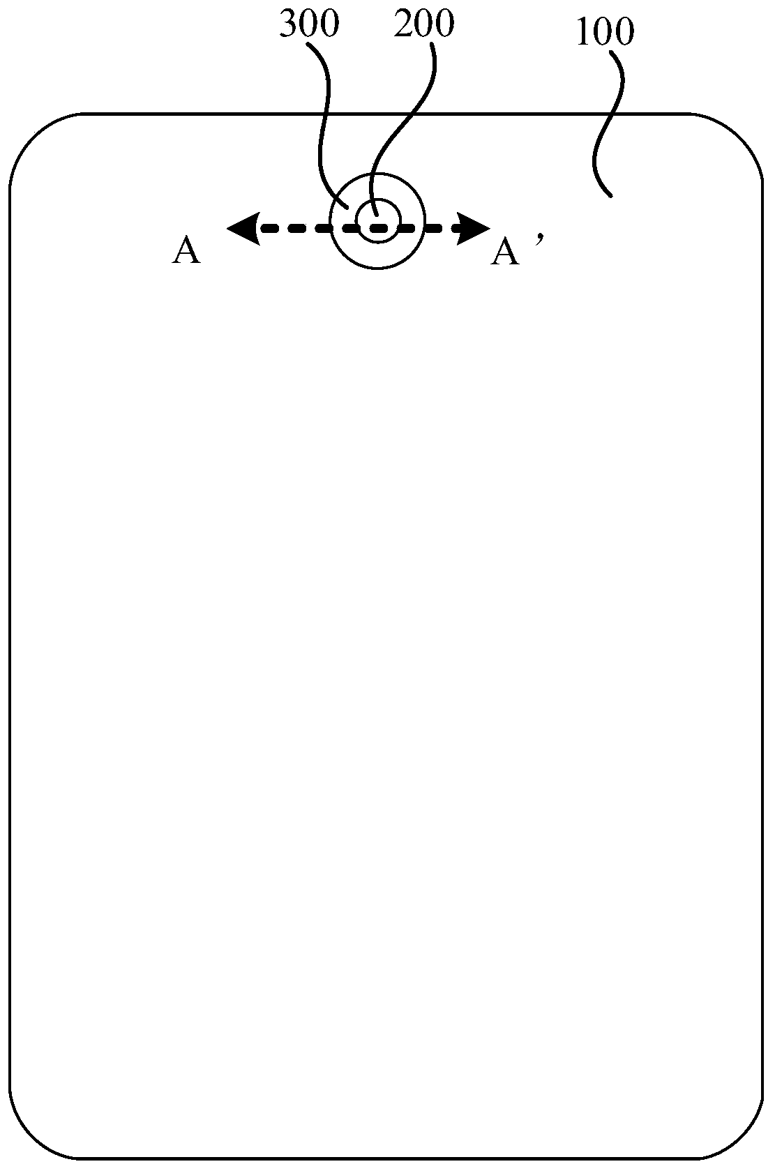
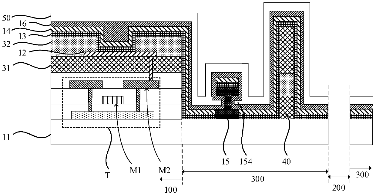
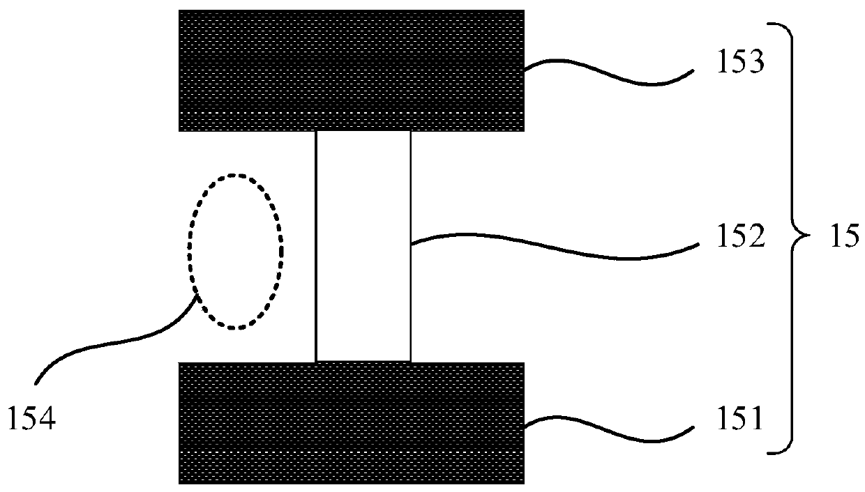
[0027] figure 1 It is a schematic top view structure diagram of an organic light emitting display panel provided by an embodiment of the present invention, figure 2 for along figure 1 Schematic diagram of the cross-sectional structure in the direction of AA', image 3 For a schematic cross-sectional structure diagram of a segmented part provided by an embodiment of the present invention, refer to figure 1 , figure 2 with image 3 , the organic light emitting display panel includes a display area 100 , a via...
PUM
 Abstract
Description
Claims
Application Information
 - R&D
- Intellectual Property
- Life Sciences
- Materials
- Tech Scout
- Unparalleled Data Quality
- Higher Quality Content
- 60% Fewer Hallucinations
Browse by: Latest US Patents, China's latest patents, Technical Efficacy Thesaurus, Application Domain, Technology Topic, Popular Technical Reports.
© 2025 PatSnap. All rights reserved.Legal|Privacy policy|Modern Slavery Act Transparency Statement|Sitemap|About US| Contact US: help@patsnap.com