Biodegradable baseplate used for soft light electron device and manufacturing method thereof

A kind of optoelectronic device, flexible technology, applied in semiconductor/solid-state device manufacturing, electric solid-state device, photovoltaic power generation, etc., can solve the problem of poor surface smoothness of flexible substrates

Inactive Publication Date: 2015-07-08
UNIV OF ELECTRONIC SCI & TECH OF CHINA
View PDF8 Cites 8 Cited by
  • Summary
  • Abstract
  • Description
  • Claims
  • Application Information

AI Technical Summary

Problems solved by technology

[0005] In order to solve the above technical problems, the present invention provides a biodegradable substrate for flexible optoelectronic devices and its manufacturing method, which solves the problem of poor surface smoothness of the flexible substrate and improves the barrier ability of the flexible substrate to water and oxygen , improve the adhesion of

Method used


Image

  • Biodegradable baseplate used for soft light electron device and manufacturing method thereof
  • Biodegradable baseplate used for soft light electron device and manufacturing method thereof
  • Biodegradable baseplate used for soft light electron device and manufacturing method thereof

Examples


Embodiment 1

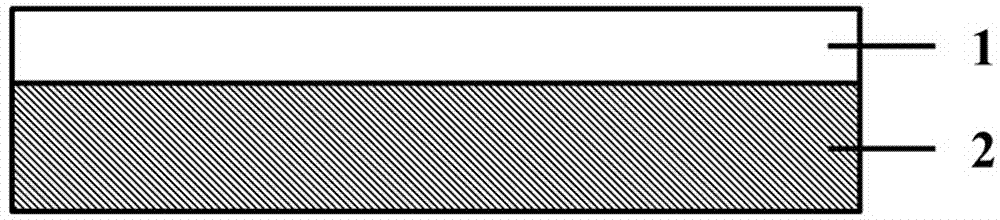
[0168] Such as figure 1In the substrate structure shown, the flexible substrate 2 is shellac mixed with dual-curing adhesive, the dual-curing adhesive adopts a dual-curing system of free radical ultraviolet curing agent-thermal curing agent, and the conductive layer 1 is an ITO film.

[0169] The preparation method is as follows:

[0170] ①Use detergent, acetone solution, ethanol solution and deionized water to ultrasonically clean the glass substrate, and dry it with dry nitrogen after cleaning;

[0171] ② Stir the mixed solution of shellac-dual curing glue (dual curing glue accounted for 0.3% by mass) diluted 1:10 with ethanol for 20 hours, then spin-coat it on the surface of the glass substrate with a film thickness of about 100 microns;

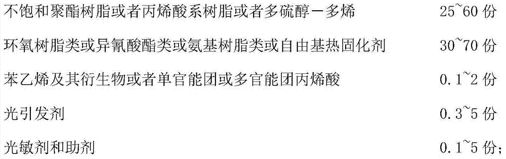
[0172] Wherein the proportioning ratio of dual curing rubber raw material components is:

[0173]

[0174] ③UV curing treatment on the surface of the substrate for 30 seconds;

[0175] ④Put the substrate into the oven at a temperatu...

Embodiment 2

[0181] Such as figure 1 In the substrate structure shown, the flexible substrate 2 is shellac mixed with dual-curing adhesive, the dual-curing adhesive adopts a dual-curing system of free radical ultraviolet curing agent-microwave curing agent, and the conductive layer 1 is carbon nanotubes.

[0182] The preparation method is as follows:

[0183] ①Use detergent, acetone solution, ethanol solution and deionized water to ultrasonically clean the glass substrate, and dry it with dry nitrogen after cleaning;

[0184] ② Stir the mixed solution of shellac-dual curing glue (dual curing glue accounted for 0.4% by mass) diluted 1:10 with ethanol for 20 hours, then spin-coat it on the surface of the glass substrate with a film thickness of about 300 microns;

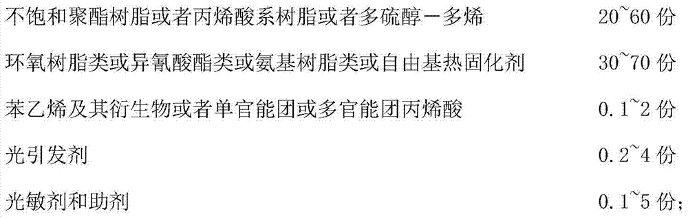
[0185] Wherein the proportioning ratio of dual curing rubber raw material components is:

[0186]

[0187] ③The substrate obtained in step ② is treated with ultraviolet light, and the treatment time is 30s;

[0188] ④ Put th...

Embodiment 3

[0194] Such as figure 1 In the substrate structure shown, the flexible substrate 2 is shellac mixed with dual-curing adhesive, the dual-curing adhesive adopts a dual-curing system of free radical ultraviolet curing agent-anaerobic curing agent, and the conductive layer 1 is silver nanowires.

[0195] The preparation method is as follows:

[0196] ① Clean the glass substrate with a surface roughness less than 1nm first, then use detergent, acetone, deionized water, and isopropanol to perform ultrasonic cleaning, and then dry it with dry nitrogen after cleaning;

[0197] ② Stir the mixed solution of shellac-dual curing glue (dual curing glue accounted for 0.5% by mass) diluted 1:10 with ethanol for 20 hours, then spin-coat it on the surface of the glass substrate, with a film thickness of about 500 microns;

[0198] Wherein the proportioning ratio of dual curing rubber raw material components is:

[0199]

[0200] ③UV curing the substrate obtained in step ② for 40 seconds; ...


PUM

PropertyMeasurementUnit
Surface roughnessaaaaaaaaaa
Thicknessaaaaaaaaaa
Thicknessaaaaaaaaaa

Abstract

The invention discloses a biodegradable baseplate used for a soft light electron device and a manufacturing method thereof. The baseplate comprises a flexible substrate and a conducting layer, the conducting layer is located on the flexible substrate, the flexible substrate is made of lac mixed with dual curing glue, the mass ratio of the dual curing glue in the lac is 0.3 - 4%, the dual curing glue is composed of a dual curing system, and the dual curing system is an ultraviolet curing-thermocuring system, an ultraviolet curing-micro curing system, an ultraviolet curing-anaerobic curing system or an ultraviolet curing-electron beam curing system. According to the substrate, after the dual curing treatment, the molecules are crosslinked with one another, the resin molecules in the lac are prevented from crystallization, the light scattering is reduced, the light transmittance of the flexible substrate is improved, the performance of the soft light electron device is improved, and meanwhile the problem that the flexibility of the substrate is not high is solved, the obstructing capacity to water radon of the flexible substrate and the smoothness of the surface of the substrate are promoted, and the affinity between a conductive film and the substrate is improved.

Description

technical field [0001] The invention belongs to the technical field of organic optoelectronics, and in particular relates to a degradable substrate for flexible optoelectronic devices and a manufacturing method thereof. Background technique [0002] With the wide application of optoelectronic technology in optoelectronic products such as solar cells, optical image sensors, plasma flat panel displays, electroluminescent displays, thin film transistors, and liquid crystal display panels, the optoelectronic information industry has received more and more attention from various countries and has become One of the important development areas, the competition in the field of optoelectronic information is also intensifying. Although traditional rigid substrates (such as glass or silicon wafers) have excellent device performance, they are weak in vibration and impact resistance, relatively heavy in weight, and not easy to carry, which is greatly limited in application. In the past ...

Claims


Application Information

Patent Timeline
IPC IPC(8): H01L51/52H01L51/54H01L51/56
CPCH10K77/111Y02E10/549
Inventor 于军胜范惠东王煦施薇
Owner UNIV OF ELECTRONIC SCI & TECH OF CHINA
Why Eureka
Try Eureka