Light-emitting device and method for manufacturing the same

a technology of light-emitting devices and manufacturing methods, applied in the field of light-emitting elements, to achieve the effect of prolonging the li

Active Publication Date: 2010-04-22
SEMICON ENERGY LAB CO LTD
View PDF15 Cites 46 Cited by
  • Summary
  • Abstract
  • Description
  • Claims
  • Application Information

AI Technical Summary

Benefits of technology

[0011]Such the light-emitting element can suppress crystallization of a layer containing one compound selected from the group consisting of oxide semiconductor and a metal oxide, and a compound having high hole transportation properties. As a result, a lifetime of a light-emitting element can be extended.
[0016]Such the light-emitting element that includes a layer containing one compound selected from the group consisting of oxide semiconductor and a metal oxide, a compound having high hole transportation properties, and a compound having a high steric hindrance can suppress the crystallization of the layer. As a result, a lifetime of a light-emitting element can be extended.
[0019]According to the present invention, aggregation of oxide semiconductor or a metal oxide can be suppressed, and crystallization of a layer containing the oxide semiconductor or the metal oxide can be suppressed. By suppression of the crystallization, a leak current can be prevented from generating due to the crystallization. Accordingly, a long-lived light-emitting element can be obtained.

Problems solved by technology

The means for extending a lifetime of a light-emitting element disclosed in the unexamined patent publication No. 9-63771 is insufficient, and so it is required to develop the technique for achieving a further long lifetime.

Method used


Image

  • Light-emitting device and method for manufacturing the same
  • Light-emitting device and method for manufacturing the same
  • Light-emitting device and method for manufacturing the same

Examples


example 1

[0057]Hereinafter, a method for manufacturing a light-emitting element according to the present invention and properties of the light-emitting element is explained.

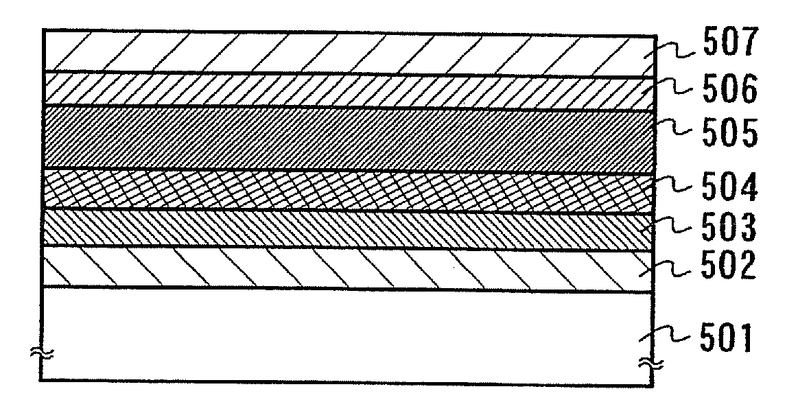
[0058]A first electrode is formed by depositing an indium tin oxide (ITO) over a glass substrate. Then, the glass substrate deposited with the ITO is processed in vacuum at 150° C. for 30 minutes.

[0059]A first layer is formed by co-evaporation of a molybdenum oxide and α-NPD having high hole transporting properties over the first electrode. The weight ratio of the molybdenum oxide and the α-NPD is 0.245:1. The first layer is formed to have a thickness of 130 nm. As used herein, the term “co-evaporation” refers to a method for evaporating each of materials from a plurality of evaporation sources provided in one processing chamber, and mixing the evaporated materials in the gas phase to deposit the mixed materials onto a subject.

[0060]A second layer is formed by vapor deposition of α-NPD over the first layer to have a thick...

example 2

[0068]A method for manufacturing a light-emitting element according to the present invention and characteristics of the light-emitting element is explained.

[0069]A first electrode is formed by depositing an indium tin oxide (ITO) over a glass substrate. The glass substrate deposited with the ITO is processed in vacuum at 150° C. for 30 minutes.

[0070]A first layer is formed over the first electrode by co-evaporation of a molybdenum oxide, α-NPD having high hole transportation properties, and rubrene having a high steric hindrance. The weight ratio of the molybdenum oxide and the rubrene is 0.245:0.018. The first layer is formed to have a thickness of 130 nm.

[0071]A second layer is formed by vapor deposition α-NPD over the first layer to have a thickness of 10 nm.

[0072]A third layer is formed over the second layer by co-evaporation of Alq3 and coumarin-6 to have a thickness of 37.5 nm. The weight ratio of the Alq3 and the coumarin-6 is 1:0.002.

[0073]A fourth layer is formed by vapor d...

example 3

[0079]A method for manufacturing a light-emitting element according to the present invention and properties of the light-emitting element is explained.

[0080]A first electrode is formed by depositing an indium tin oxide (ITO) over a glass substrate. The glass substrate deposited with the ITO is processed in vacuum at 150° C. for 30 minutes.

[0081]A first layer is formed over the first electrode by co-evaporation of a molybdenum oxide, 4,4-bis(N-(4-(N,N-di-m-trylamino)phenyl)-N-phenylamino)biphenyl (abbreviated DNTPD) having high hole transportation properties, and rubrene having a high steric hindrance. The weight ratio of the molybdenum oxide, the DNTPD, and the rubrene is 0.5:1:0.05. The first layer is formed to have a thickness of 120 nm.

[0082]A second layer is formed by vapor deposition of α-NPD over the first layer to have a thickness of 10 nm.

[0083]A third layer is formed over the second layer by co-evaporation of Alq3 and coumarin-6 to have a thickness of 37.5 nm. The weight ra...


PUM


Abstract

A light-emitting element is disclosed that can drive at a low driving voltage and that has a longer lifetime than the conventional light-emitting element, and a method is disclosed for manufacturing the light-emitting element. The disclosed light-emitting element includes a plurality of layers between a pair of electrodes; and at least one layer among the plurality of layers contains one compound selected from the group consisting of oxide semiconductor and a metal oxide, and a compound having high hole transportation properties. Such the light-emitting element can suppress the crystallization of a layer containing one compound selected from the group consisting of oxide semiconductor and a metal oxide, and a compound having high hole transportation properties. As a result, a lifetime of the light-emitting element can be extended.

Description

TECHNICAL FIELD[0001]The present invention relates to a light-emitting element formed to have the structure in which a plurality of layers is sandwiched between a pair of electrodes. More specifically, the present invention relates to the structure of a layer, which can be used as at least one layer, within the plurality of layers.BACKGROUND ART[0002]A light-emitting device utilizing light emission from an electroluminescent element (light-emitting element) has been attracted attention as a display device or a lighting device.[0003]As a light-emitting element used for a light-emitting device, a light-emitting element including a layer containing light-emitting compounds interposed between a pair of electrodes is well known.[0004]Within such a light-emitting element, either of the electrodes serves as an anode, and another serves as a cathode, holes injected from the anode and electrons injected from the cathode are recombined with each other to form molecular exciton, and the molecu...

Claims


Application Information

Patent Timeline
Patent Type & Authority Applications(United States)
IPC IPC(8): H01L51/54H01L29/22H01LH05B33/10H05B33/14H05B33/22
CPCH01L51/5088H01L51/5048H10K50/14H10K50/17
Inventor IKEDA, HISAOSAKATA, JUNICHIRO
Owner SEMICON ENERGY LAB CO LTD
Why Eureka
Try Eureka