Semiconductor structure and method for forming same

A semiconductor and isolation structure technology, which is applied in semiconductor devices, semiconductor/solid-state device manufacturing, semiconductor/solid-state device components, etc., can solve problems such as poor chip performance and single function, and achieve the effect of reducing damage

Inactive Publication Date: 2019-05-31
HUAIAN IMAGING DEVICE MFGR CORP
View PDF8 Cites 3 Cited by
  • Summary
  • Abstract
  • Description
  • Claims
  • Application Information

AI Technical Summary

Problems solved by technology

[0004] However, the function of the existing sealing ring structure is relatively single, so the performance of the chip formed by dicing is still poor

Method used


Image

  • Semiconductor structure and method for forming same
  • Semiconductor structure and method for forming same
  • Semiconductor structure and method for forming same

Examples


Embodiment Construction

[0025] As mentioned in the background art, the function of the existing sealing ring structure is relatively single.

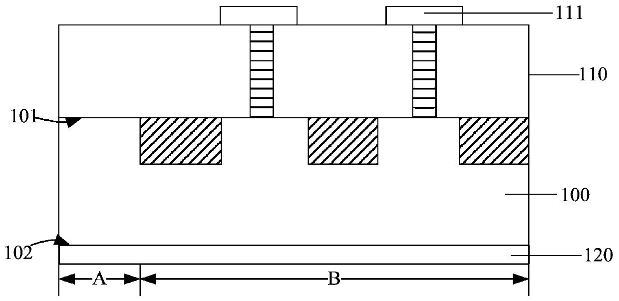
[0026] figure 1 A schematic diagram of a semiconductor structure.

[0027] Please refer to figure 1 , a substrate 100, the substrate 100 includes several device regions A and several seal ring regions B, and each device region A is respectively surrounded by the seal ring region B, the substrate 100 includes an opposite first surface 101 and a second Surface 102; the first device layer 110 located on the surface of the first surface 101 of several device regions A and several seal ring regions B of the substrate 100, the first device layer 110 includes the surface of the first surface 101 of the seal ring region B of the substrate 100 the first conductive layer 111; the second conductive layer 120 on the surface of the second surface 102 of the sealing ring region B of the substrate 100.

[0028] In the above-mentioned semiconductor structure, during the pr...


PUM


Abstract

A semiconductor structure and a method for forming the same are disclosed. The semiconductor structure comprises a first substrate including a plurality of device regions and a plurality of sealing ring regions, wherein each device region is surrounded by the corresponding sealing ring region, and the first substrate includes opposing first and second faces; a first device layer located on the surface of the first face of the plurality of device regions and the plurality of sealing ring regions of the first substrate and including a first conductive layer on the surface of the first face of the sealing ring regions of the first substrate; a first plug located in the sealing ring regions of the first substrate and electrically connected to the first conductive layer, wherein the second faceof the first substrate exposes the first plug; and a second conductive layer on the surface of the second face of the sealing ring regions of the first substrate and connected to the first plug. Thesemiconductor structure has a shielding and antistatic effect.

Description

technical field [0001] The invention relates to the field of semiconductor manufacturing, in particular to a semiconductor structure and a forming method thereof. Background technique [0002] In the manufacture of an integrated circuit (IC, Integrated Circuit), making a sealing ring (also called a protective ring, Seal Ring) is an important part of the semiconductor process. [0003] With the development of semiconductor technology, integrated circuits are made in the form of chips. A scribe line exists between adjacent chips on the wafer, and the wafer is cut through the scribe line to divide the wafer into multiple chips. However, during the process of dicing the wafer, mechanical stress is easily generated, and the mechanical stress is likely to cause damage to the chip. In order to prevent the semiconductor chip from being damaged by the dicing process, a seal ring structure is formed between the chip and the scribe line. [0004] However, the function of the existin...

Claims


Application Information

Patent Timeline
Patent Type & Authority Applications(China)
IPC IPC(8): H01L23/02H01L23/552H01L23/60H01L21/60
CPCH01L2224/08145
Inventor 何延强林宗德黄仁德汪旭东
Owner HUAIAN IMAGING DEVICE MFGR CORP
Why Eureka
Try Eureka