Check patentability & draft patents in minutes with Patsnap Eureka AI!

Circuit of multi-bus reconfigurable processor chip

A processor, multi-bus technology, applied in electrical program control, program control in sequence/logic controllers, etc., to achieve low power consumption, high-performance data processing capabilities, and meet the needs of miniaturization.

Inactive Publication Date: 2019-06-04
XIAN AVIATION COMPUTING TECH RES INST OF AVIATION IND CORP OF CHINA
View PDF5 Cites 0 Cited by
  • Summary
  • Abstract
  • Description
  • Claims
  • Application Information

AI Technical Summary

Problems solved by technology

[0002] The flight control system of the airborne computer needs to be equipped with a high-performance processor, embedded with a large-capacity FPGA, which can realize function customization, and at the same time realize the communication between the flight control computer and peripherals through 429, 422, 1553B and other interfaces. The required processor chip

Method used


Image

  • Circuit of multi-bus reconfigurable processor chip
  • Circuit of multi-bus reconfigurable processor chip

Examples


Embodiment Construction

[0016] The present invention will be further described below in conjunction with accompanying drawing and embodiment:

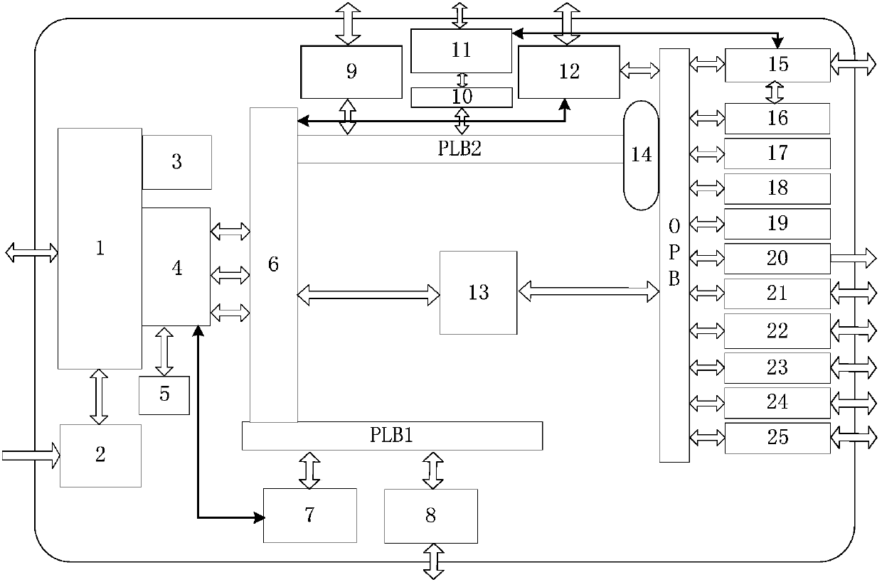
[0017] see figure 1 The multi-bus reconfigurable processor chip circuit structure of the present invention includes a processor core, an interrupt controller, a floating-point processing unit, a secondary Cache controller, an SRAM memory, a PLB arbiter, an SRAM controller, an SDRAM controller, and a 1553B protocol Processor, FPGA core interface, FPGA core, Ethernet interface, DMA controller, PLB to OPB bridge, FPGA core loading circuit, EBC memory interface, watchdog, timer, real-time clock, pulse width modulation, LVDS interface, 429 Bus controller, serial port controller, IIC interface and general input and output modules. The processor core is directly connected to the interrupt controller, the floating-point processing unit, and the secondary cache controller. The secondary cache controller is directly connected to the SRAM memory and the PLB arbiter. Th...


PUM


Abstract

The invention belongs to a computer hardware technology, and relates to a circuit structure of a multi-bus reconfigurable processor chip. The circuit comprises an FPGA core, a bus, an FPGA core interface and an FPGA core loading circuit. The FPGA core is programmable, the processor accesses the FPGA core by means of the bus and the FPGA core interface, and the user loads an independently designedlogic circuit into the FPGA core by means of the FPGA core loading circuit. The circuit of the multi-bus reconfigurable processor chip is provided.

Description

technical field [0001] The invention belongs to computer hardware technology and relates to a circuit structure of a multi-bus reconfigurable processor chip. Background technique [0002] The flight control system of the airborne computer needs to be equipped with a high-performance processor, embedded with a large-capacity FPGA, which can realize function customization, and at the same time realize the communication between the flight control computer and peripherals through 429, 422, 1553B and other interfaces. The required processor chip. Contents of the invention [0003] The purpose of the present invention is to provide a multi-bus reconfigurable processor chip circuit. [0004] Technical solution of the present invention: a multi-bus reconfigurable processor chip circuit, characterized in that: the circuit includes an FPGA core, a bus, an FPGA core interface and an FPGA core loading circuit, and the FPGA core is programmable, processing The device accesses the FPG...

Claims


Application Information

Patent Timeline
Patent Type & Authority Applications(China)
IPC IPC(8): G05B19/05
Inventor 刘承禹田泽郭蒙王泉杜斐王世中
Owner XIAN AVIATION COMPUTING TECH RES INST OF AVIATION IND CORP OF CHINA
Features
  • R&D
  • Intellectual Property
  • Life Sciences
  • Materials
  • Tech Scout
  • Unparalleled Data Quality
  • Higher Quality Content
  • 60% Fewer Hallucinations
Learn More