Array substrate, manufacturing method of array substrate, liquid crystal display device and driving method of liquid crystal display device

A technology of liquid crystal display devices and array substrates, applied in nonlinear optics, instruments, optics, etc., can solve the problems of narrow viewing angle dark state light leakage contrast, reduction, etc., and achieve the effect of preventing dark state light leakage

Active Publication Date: 2019-06-07
KUSN INFOVISION OPTOELECTRONICS
View PDF12 Cites 2 Cited by
  • Summary
  • Abstract
  • Description
  • Claims
  • Application Information

AI Technical Summary

Problems solved by technology

[0006] In order to overcome the shortcomings and deficiencies existing in the prior art, the purpose of the present invention is to provide an array substrate and its manufacturing method, a liquid crystal display device and its driving method, so as to solve the problem of light leakage and reduced contrast in the narrow viewing angle dark state

Method used


Image

  • Array substrate, manufacturing method of array substrate, liquid crystal display device and driving method of liquid crystal display device
  • Array substrate, manufacturing method of array substrate, liquid crystal display device and driving method of liquid crystal display device
  • Array substrate, manufacturing method of array substrate, liquid crystal display device and driving method of liquid crystal display device

Examples


Embodiment 1

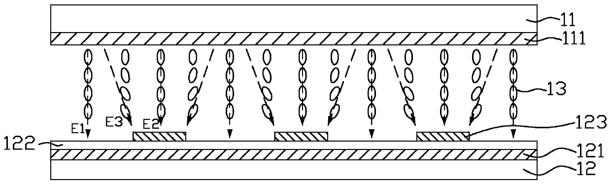
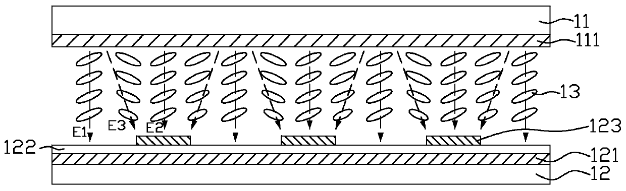
[0043] Figure 4 It is a schematic cross-sectional structure diagram of a liquid crystal display device in a wide viewing angle dark state in Embodiment 1 of the present invention, Figure 5 It is a schematic diagram of the cross-sectional structure of the liquid crystal display device in the embodiment 1 of the present invention when it is in a bright state with a wide viewing angle, Image 6 It is a schematic diagram of the cross-sectional structure of the liquid crystal display device in the narrow viewing angle dark state in Embodiment 1 of the present invention, Figure 7 It is a schematic diagram of the cross-sectional structure of the liquid crystal display device in Embodiment 1 of the present invention when it is in a bright state with a narrow viewing angle. Please refer to Figure 4 to Figure 7 Embodiment 1 of the present invention also provides a liquid crystal display device, including an array substrate 30 , a color filter substrate 20 disposed opposite to the ...

Embodiment 2

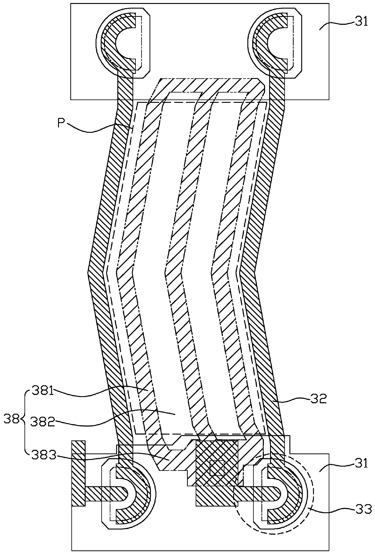
[0064] Figure 10 It is a schematic cross-sectional structure diagram of the liquid crystal display device in the second embodiment of the present invention in a bright state with a narrow viewing angle. Please refer to Figure 10 , the liquid crystal display panel provided by the second embodiment of the present invention is the same as that of the first embodiment ( Figure 7 The structure and working principle of the liquid crystal display panel in ) are basically the same, the difference is that in this embodiment, the thickness of the second insulating layer 37 above the plurality of insulating protrusions 35 is smaller than that of the second insulating layer 37 above the plurality of electrodes. Thickness above flat 362. For example, the thickness of the second insulating layer 37 above the plurality of insulating protrusions 35 may be zero to reduce the influence of the second insulating layer 37 on the vertical electric field formed between the common electrode 36 a...

Embodiment 3

[0071] Figure 11 It is a schematic cross-sectional structure diagram of the liquid crystal display device in the third embodiment of the present invention in a bright state with a narrow viewing angle. Please refer to Figure 11 , the liquid crystal display panel provided by the third embodiment of the present invention is the same as that of the first embodiment ( Figure 7The structure and working principle of the liquid crystal display panel in ) are basically the same, the difference is that in this embodiment, the height of the upper surfaces of the plurality of electrode protrusions 361 in the same horizontal direction is higher than that of the upper surfaces of the plurality of pixel electrode strips 381 the height of. Improve the shielding effect of the electrode protrusions 361 on the partial electric field at the edge of the pixel electrode strips 381 in the horizontal direction, so that a vertical and evenly distributed electric field is formed between the array...


PUM


Abstract

The invention discloses an array substrate. The array substrate comprises a flat layer, a first insulating layer, a common electrode, a second insulating layer and a pixel electrode, wherein the flatlayer, the first insulating layer, the common electrode, the second insulating layer and the pixel electrode are sequentially arranged on the array substrate, the pixel electrode is of a comb structure with a plurality of pixel electrode strips and a plurality of slits which are alternately arranged; the first insulating layer is of a patterned structure and comprises a plurality of insulating protrusions which correspond to the slits; the insulating protrusions extend in the same direction with the pixel electrode strips and are alternately arranged in a pixel unit; and the common electrode forms a plurality of electrode convex parts above the insulating protrusions and a plurality of electrode flat parts below the pixel electrode strips. The invention further discloses a manufacturing method of the array substrate. The invention further discloses a liquid crystal display device, the liquid crystal display device comprises the array substrate, a color film substrate and a liquid crystal layer positioned between the color film substrate and the array substrate. The invention further discloses a driving method of the liquid crystal display device.

Description

technical field [0001] The invention relates to the technical field of liquid crystal display, in particular to an array substrate and a manufacturing method, a liquid crystal display device and a driving method. Background technique [0002] Liquid crystal display (LCD) has the advantages of good picture quality, small size, light weight, low driving voltage, low power consumption, no radiation and relatively low manufacturing cost, and it occupies a dominant position in the field of flat panel display. [0003] With the continuous advancement of liquid crystal display technology, the viewing angle of the display has been expanded from about 120° to more than 160°. While enjoying the visual experience brought by the large viewing angle, people also hope to effectively protect commercial secrets and personal privacy. Avoid commercial loss or embarrassment caused by information leakage on the screen. Therefore, in addition to wide viewing angles, there is also a need for dis...

Claims


Application Information

Patent Timeline
IPC IPC(8): G02F1/1343
Inventor 沈家军钟德镇乔艳冰姜丽梅
Owner KUSN INFOVISION OPTOELECTRONICS
Why Eureka
Try Eureka