Array substrate, preparation method of array substrate, display panel, and display device

A technology of array substrates and substrate substrates, which is applied in the direction of electrical components, electric solid devices, circuits, etc., can solve the problems of being unable to simultaneously realize gray scale and effective control of switches, and achieve the effects of low cost, guaranteed switching performance, and simple process

Inactive Publication Date: 2019-06-11
BOE TECH GRP CO LTD +1
View PDF5 Cites 5 Cited by
  • Summary
  • Abstract
  • Description
  • Claims
  • Application Information

AI Technical Summary

Problems solved by technology

Both of the current display products use the same design, that is, the sub-threshold swings of the driving transistor and the s

Method used


Image

  • Array substrate, preparation method of array substrate, display panel, and display device
  • Array substrate, preparation method of array substrate, display panel, and display device
  • Array substrate, preparation method of array substrate, display panel, and display device

Examples


preparation example Construction

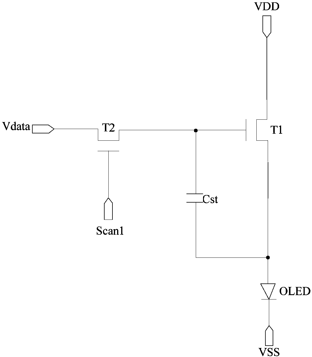
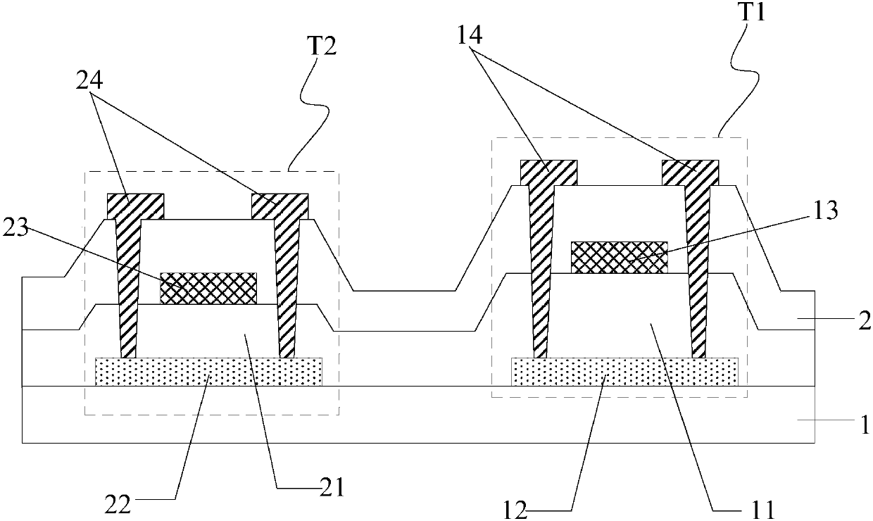
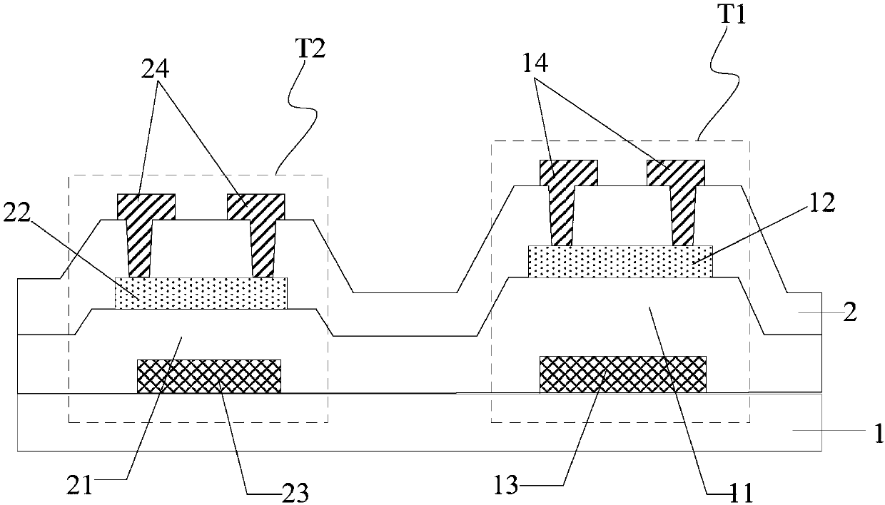
[0071] In the preparation method of the array substrate provided by the embodiment of the present invention, the thickness of the gate oxide layer of the driving transistor is greater than the thickness of the gate oxide layer of the switching transistor, according to I=K(Vgs-Vth) 2 ,as well as The thickness of the gate oxide layer of the driving transistor is greater than the thickness of the gate oxide layer of the switching transistor, which is equivalent to the K of the driving transistor being smaller than the K of the switching transistor, so that the change of the current of the driving transistor with the voltage is small, that is, the subthreshold swing The requirement is larger in order to better control the gray scale; while the current of the switching transistor varies greatly with the voltage, that is, the subthreshold swing requirement is smaller to ensure the switching performance. At the same time, the effective control of the gray scale and switch in the dis...


PUM

PropertyMeasurementUnit
Thicknessaaaaaaaaaa
Thicknessaaaaaaaaaa

Abstract

The invention discloses an array substrate, a preparation method of the array substrate, a display panel, and a display device. The array substrate is characterized in that the thickness of a gate oxidation layer of a driving transistor is larger than the thickness of a gate oxidation layer of a switching transistor. According to I=K(Vgs-Vth)<2> and (the formula is as shown in the description), the fact that the thickness of the gate oxidation layer of the driving transistor is larger than the thickness of the gate oxidation layer of the switching transistor indicates that K of the driving transistor is smaller than K of the switching transistor, so that current changes of the driving transistor with voltages are smaller, i.e., subthreshold swing requirements are higher, which facilitatesbetter grayscale control, and current changes of the switching transistor with the voltages are larger, i.e., subthreshold swing requirements are lower, which ensures good switching performance; and therefore, effective grayscale and switching control in the display panel can be simultaneously achieved.

Description

technical field [0001] The invention relates to the field of display technology, in particular to an array substrate, a preparation method thereof, a display panel and a display device. Background technique [0002] Organic Light Emitting Diode (OLED) display devices have gradually occupied the application markets of smartphones, smart wearables, and TVs due to their advantages such as high contrast, ultra-fast response, bright colors, easy thinning, and flexibility. However, OLED display devices are all current-driven devices. When the current varies too drastically with the voltage, the display gray scale is difficult to control, and even different types of mura appear due to uneven current, which seriously affects the display effect. [0003] In an OLED display device, a pixel circuit for driving the OLED to emit light includes a driving transistor and a switching transistor. The driving transistor requires a small change in current with voltage, that is, a larger sub-th...

Claims


Application Information

Patent Timeline
IPC IPC(8): H01L27/12H01L27/32
Inventor 白妮妮康峰刘亮亮
Owner BOE TECH GRP CO LTD
Why Eureka
Try Eureka