Display panel and preparation method thereof

A technology for display panels and substrates, applied in instruments, semiconductor devices, computing, etc., can solve the problems that OLED display panels cannot achieve fingerprint recognition, liquid crystal display panels cannot achieve off-screen fingerprint recognition, and high requirements for optical path structure and size design, and achieve improved performance. The production yield, not easy to warp, and the effect of reducing production costs

Inactive Publication Date: 2021-07-09
WUHAN CHINA STAR OPTOELECTRONICS TECH CO LTD
View PDF9 Cites 1 Cited by
  • Summary
  • Abstract
  • Description
  • Claims
  • Application Information

AI Technical Summary

Problems solved by technology

[0007] The purpose of the present invention is to provide a display panel and a preparation method thereof to solve the problem that in the prior art, the liquid crystal display panel cannot realize fingerprint recognition under the screen, the OLED display panel cannot realize full-screen and full-area fingerprint recognition, and the existing fingerprint recognition technology is difficult The size design requirements of the optical path structure are relatively high, there are many limiting factors, and it is difficult to realize ultra-thin, high-resolution fingerprint recognition screen and other technical problems

Method used


Image

  • Display panel and preparation method thereof
  • Display panel and preparation method thereof
  • Display panel and preparation method thereof

Examples


Embodiment 1

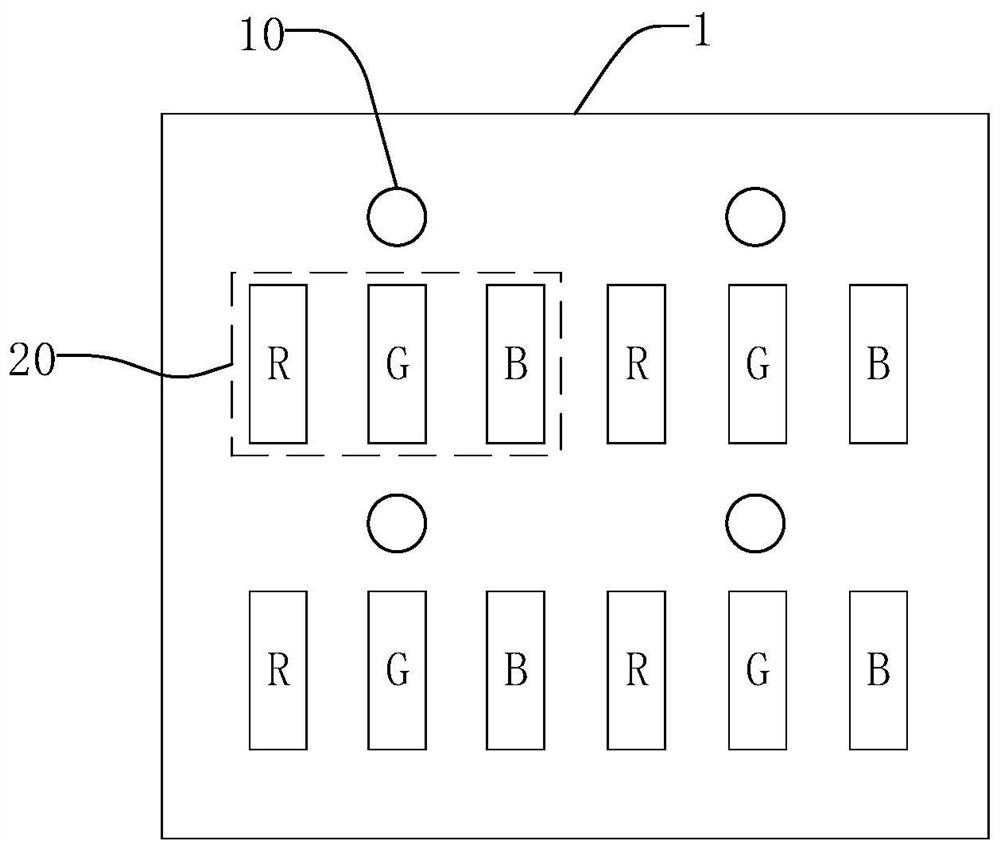
[0054] An embodiment of the present invention provides a display panel 1, such as figure 1 As shown, several pixel units 20 and several fingerprint recognition units 10 are evenly distributed in the display panel 1 . The pixel unit 20 has a red sub-pixel R, a green sub-pixel G, and a blue sub-pixel B arranged in sequence, and the fingerprint recognition unit 10 is arranged so that the green sub-pixel G is far away from the red sub-pixel R and the blue sub-pixel. One end of the blue subpixel B.

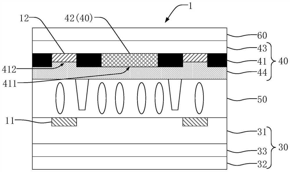
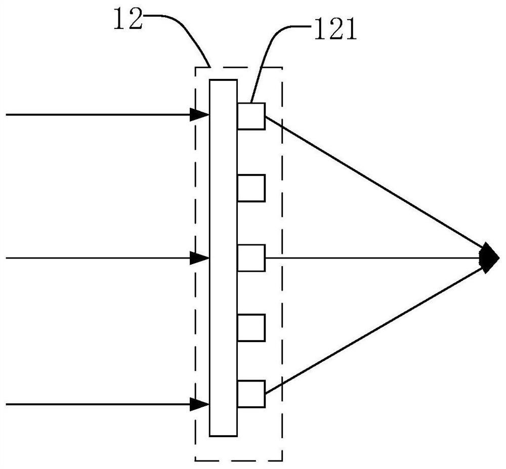
[0055] Such as figure 2As shown, the display panel 1 includes a first substrate 30 , a second substrate 40 and a liquid crystal layer 50 stacked in layers, wherein the liquid crystal layer 50 is arranged between the first substrate 30 and the second substrate 40 . The fingerprint identification unit 10 includes a sensor 11 and a metalens 12 . The sensor 11 is disposed on the first substrate 30 . The metalens 12 is disposed in the second substrate 40 and corresponding to the senso...

Embodiment 2

[0074] An embodiment of the present invention provides a display panel 1, such as figure 1 As shown, several pixel units 20 and several fingerprint recognition units 10 are evenly distributed in the display panel 1 . The pixel unit 20 has a red sub-pixel R, a green sub-pixel G, and a blue sub-pixel B arranged in sequence, and the fingerprint recognition unit 10 is arranged so that the green sub-pixel G is far away from the red sub-pixel R and the blue sub-pixel. One end of the blue subpixel B.

[0075] Such as Figure 7 As shown, the display panel 1 includes a first substrate 30 , a second substrate 40 and a liquid crystal layer 50 stacked in layers, wherein the liquid crystal layer 50 is arranged between the first substrate 30 and the second substrate 40 . The fingerprint identification unit 10 includes a sensor 11 and a metalens 12 . The sensor 11 is disposed on the first substrate 30 . The metalens 12 is disposed in the second substrate 40 and corresponding to the sens...

Embodiment 3

[0091] An embodiment of the present invention provides a display panel 1, such as figure 1 As shown, several pixel units 20 and several fingerprint recognition units 10 are evenly distributed in the display panel 1 . The pixel unit 20 has a red sub-pixel R, a green sub-pixel G, and a blue sub-pixel B arranged in sequence, and the fingerprint recognition unit 10 is arranged so that the green sub-pixel G is far away from the red sub-pixel R and the blue sub-pixel. One end of the blue subpixel B.

[0092] Such as Figure 8 As shown, the display panel 1 includes a first substrate 30 , a second substrate 40 and a liquid crystal layer 50 stacked in layers, wherein the liquid crystal layer 50 is arranged between the first substrate 30 and the second substrate 40 . The fingerprint identification unit 10 includes a sensor 11 and a metalens 12 . The sensor 11 is disposed on the first substrate 30 . The metalens 12 is disposed in the second substrate 40 and corresponding to the sens...


PUM

PropertyMeasurementUnit
diameteraaaaaaaaaa

Abstract

The invention provides a display panel and a preparation method thereof. The display panel comprises a first substrate, a second substrate and fingerprint identification units, wherein the first substrate and the second substrate are arranged in a laminated mode. Each fingerprint identification unit comprises a sensor and at least one super-structure lens. The sensors are arranged in the first substrate. And the super-structure lenses are arranged in the second substrate and corresponds to the sensors.

Description

technical field [0001] The invention relates to the field of optical display devices, in particular to a display panel and a preparation method thereof. Background technique [0002] With consumers' pursuit of the ultimate screen-to-body ratio of mobile phones, full screens have become a trend in the development of high-end mobile phones, which requires some special processing of the fingerprint recognition system. In order to realize a full screen, the fingerprint identification system can be handled in the following ways: (1) placed on the back; (2) placed on the side; (3) under-screen or in-screen fingerprint identification. Due to the self-luminous characteristics of OLED (Organic Light-Emitting Diode, organic electroluminescent display), it is relatively easy to realize fingerprint recognition under the screen, and has been used in many mobile phones. However, LCD (Liquid Crystal Display, liquid crystal display) is passive light-emitting, and it is relatively difficult...

Claims


Application Information

Patent Timeline
Patent Type & Authority Applications(China)
IPC IPC(8): G02F1/1333G02F1/1335G02F1/13357H01L27/32G06K9/00
CPCG02F1/1333G02F1/133526G02F1/133512G02F1/133514G02F1/1336G06V40/1324H10K59/00
Inventor 李国鹏黄长治
Owner WUHAN CHINA STAR OPTOELECTRONICS TECH CO LTD
Why Eureka
Try Eureka