GaN-based light-emitting diode epitaxial wafer and manufacturing method thereof

A light-emitting diode, gallium nitride-based technology, applied in semiconductor devices, electrical components, circuits, etc., can solve the problems of reduced luminous efficiency and radiation recombination rate, so as to improve luminous efficiency, improve distribution uniformity, and slow down transition heat speed effect

Active Publication Date: 2020-08-18
HC SEMITEK ZHEJIANG CO LTD
View PDF6 Cites 0 Cited by
  • Summary
  • Abstract
  • Description
  • Claims
  • Application Information

AI Technical Summary

Problems solved by technology

[0005] Because the mobility of electrons is much faster than that of holes, the distribution of electrons in the existing multi-quantum well layer is very uneven, which will lead to a decrease in the radiative recombination rate of electrons and holes in the multi-quantum wells, thereby reducing the luminous efficiency of LEDs.

Method used


Image

  • GaN-based light-emitting diode epitaxial wafer and manufacturing method thereof
  • GaN-based light-emitting diode epitaxial wafer and manufacturing method thereof
  • GaN-based light-emitting diode epitaxial wafer and manufacturing method thereof

Examples


Embodiment Construction

[0030] In order to make the object, technical solution and advantages of the present invention clearer, the implementation manner of the present invention will be further described in detail below in conjunction with the accompanying drawings.

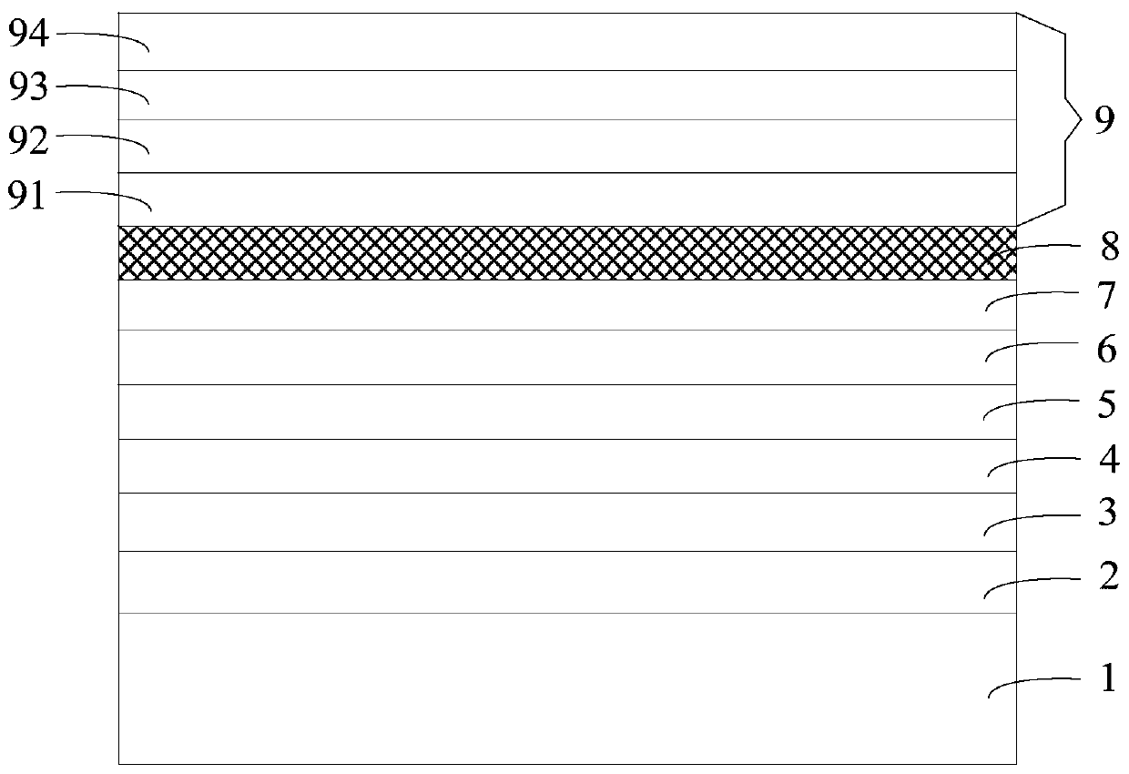
[0031] figure 1 It is a schematic structural diagram of a gallium nitride-based light-emitting diode epitaxial wafer provided by an embodiment of the present invention, as shown in figure 1 As shown, the light-emitting diode epitaxial wafer includes a substrate 1, and a low-temperature buffer layer 2, a three-dimensional nucleation layer 3, a two-dimensional recovery layer 4, an undoped GaN layer 5, and an N-type layer 6 grown on the substrate 1 in sequence. , multi-quantum well layer 8 and P-type layer 9.

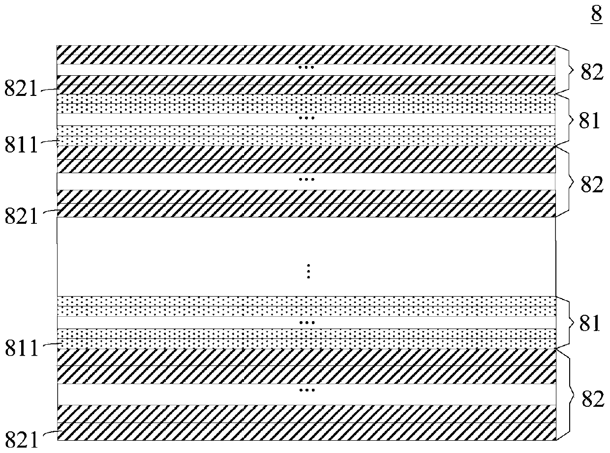
[0032] figure 2 is a schematic structural diagram of a multi-quantum well layer provided by an embodiment of the present invention, such as figure 2 As shown, the multi-quantum well layer 8 includes a plurality of periodic alt...


PUM

PropertyMeasurementUnit
thicknessaaaaaaaaaa
thicknessaaaaaaaaaa
thicknessaaaaaaaaaa

Abstract

The invention discloses a gallium nitride-based light-emitting diode epitaxial wafer and a manufacturing method thereof, and belongs to the technical field of semiconductors. A multi-quantum-well layer of the gallium nitride-based light-emitting diode epitaxial wafer comprises a plurality of quantum well layers and quantum barrier layers, wherein the quantum well layers and the quantum barrier layers are alternately grown, and each quantum well layer comprises a plurality of layers of InxGa1-xN quantum well sub-layers, wherein the In content in the plurality of layers of quantum well sub-layers is gradually increased and then gradually decreased layer by layer along the stacking direction of the epitaxial wafer; each quantum barrier layer comprises multiple layers of Si-doped ByGa1-yN quantum barrier sub-layers, wherein the B content in the plurality of layers of quantum barrier sub-layers is gradually increased and then gradually decreased layer by layer along the stacking direction of the epitaxial wafer; and x is greater than or equal to 0 and less than or equal to 1, and y is more than or equal to 0 and less than or equal to 1. According to the gallium nitride-based light-emitting diode epitaxial wafer provided by the invention, the distribution uniformity of electrons in the quantum wells can be improved, so that the radiation recombination rate of electrons and holes in the multi-quantum wells is improved, and the luminous efficiency of the LED is further improved.

Description

technical field [0001] The invention relates to the technical field of semiconductors, in particular to a gallium nitride-based light-emitting diode epitaxial wafer and a manufacturing method thereof. Background technique [0002] LED (Light Emitting Diode, Light Emitting Diode) is a semiconductor electronic component that can emit light. As an efficient, environmentally friendly and green new solid-state lighting source, it is being rapidly and widely used, such as traffic lights, car interior and exterior lights, urban landscape lighting, mobile phone backlights, etc. [0003] The epitaxial wafer is the main component of the LED. The existing GaN-based LED epitaxial wafer includes a substrate, a low-temperature buffer layer, a three-dimensional nucleation layer, a two-dimensional recovery layer, and an undoped GaN layer stacked on the substrate in sequence. , an N-type layer, a multi-quantum well layer and a P-type layer, wherein the multi-quantum well layer includes alte...

Claims


Application Information

Patent Timeline
Patent Type & Authority Patents(China)
IPC IPC(8): H01L33/06H01L33/32H01L33/00
Inventor 陶章峰乔楠刘旺平李鹏胡加辉
Owner HC SEMITEK ZHEJIANG CO LTD
Why Eureka
Try Eureka