Non-destructive measurement method of side wall angle of micro-nano scale dielectric waveguide or step structure by using confocal laser scanning microscope system

A laser scanning and microscopic system technology, which is applied in the field of precision processing and precise measurement of micro-nano optical media devices and structures, can solve the problem of inability to obtain measurement values ​​of sidewall angles, etc., achieves easy handling and placement, small size, Simple to use effects

Active Publication Date: 2021-07-09
CHANGCHUN UNIV OF SCI & TECH +1
View PDF6 Cites 0 Cited by
  • Summary
  • Abstract
  • Description
  • Claims
  • Application Information

AI Technical Summary

Problems solved by technology

In addition, it fails to obtain usable sidewall angle measurements for determining sidewall irregularities, such as those with sidewall angles close to 90° and greater than 90° (known as cliff and undercut cliffs, respectively)

Method used


Image

  • Non-destructive measurement method of side wall angle of micro-nano scale dielectric waveguide or step structure by using confocal laser scanning microscope system
  • Non-destructive measurement method of side wall angle of micro-nano scale dielectric waveguide or step structure by using confocal laser scanning microscope system
  • Non-destructive measurement method of side wall angle of micro-nano scale dielectric waveguide or step structure by using confocal laser scanning microscope system

Examples


Embodiment 1

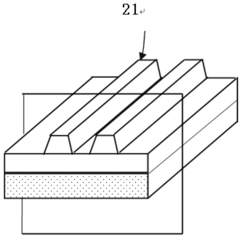
[0053] Example 1: For such as Figure 7 A reconstructed scan pattern shown in the same waveguide, select a different position to make the side corner 21 value after the cutting section, and then the average value of all selected locations is φ. ave And standard utilization value. Then using Figure 6 The measured intrinsic error is obtained. Figure 7 B The average value shown is compensated to obtain the final value. From Figure 5 B can be seen, the average of the left and right side corners φ ave From 84.90 ° and 84.83 °, respectively, by Figure 4 The given measurement error corresponds to the two angles values ​​to -1.93 ° and -1.97 °, respectively, such that the left and right sides of the measured waveguide structure are: 84.90 ° - (- 1.93 °) = 86.83 ° and 84.83 ° - (-1.97 °) = 86.80 °.

Embodiment 2

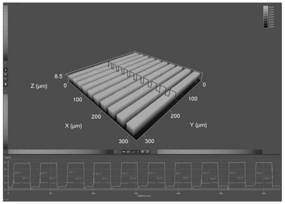
[0054] Example 2: Scanning graphics for rebuilding, such as Figure 8 A, select a plurality of waveguide channels, select one position to make the side corner 21 value after cutting the cutting section, and then evaluate all waveguide channels or structures φ ave And standard utilization value. Then using Figure 4 The measured intrinsic error is obtained. Figure 8 B The average value shown in B ave Compensation and get the final value. From Figure 8 B can be seen, the average of the left and right side corners φ ave 85.00 ° and 84.90 °, respectively, by Figure 6 The given measurement error corresponds to the two angles values ​​to -1.90 ° and -1.93 °, respectively, such that the left and right sides of the measured waveguide structure are: 85.00 ° - (- 1.90 °) = 86.90 ° and 84.90 ° - (-1.93 °) = 86.83 °.


PUM

PropertyMeasurementUnit
wavelengthaaaaaaaaaa

Abstract

The method of using a confocal laser scanning microscope system for rapid non-destructive testing of micro-nano dielectric waveguides and stepped structures involves the field of precision processing and testing. The method includes designing a confocal laser scanning microscope system, setting an adjustable pinhole diaphragm in front of the detector; designing a laser scanner with a scanning range of up to 100 microns and a control accuracy of up to 10 nanometers, and the object distance and inclination angle All adjustable stage, select 405nm wavelength laser; place the substrate to be tested on the stage, set the aperture pinhole to a value of <1.0 Airy unit, select the scanning range and scanning layer thickness Then scan and store the data; reconstruct the scan image, and test the side wall angle across the waveguide channel; calculate the average value and root mean square difference of the side wall angles of multiple channels in the channel, and calculate each The mean and root mean square difference of the sidewall angles of all cut faces on a waveguide channel. This method can be used for non-destructive online rapid detection of large-scale micro-nano structures in production.

Description

Technical field [0001] The present invention relates to the field of precision machining and precise measurement of micronine-based optical dielectric devices and structures, and more particularly to non-destructive measurement methods of micro-focus laser scanning micro-system on micro-nanometer medium waveguide or stepped structural side corner angle. Background technique [0002] As the current most mature planar optical wave line (PLC) technology, the device based on the silicon oxide waveguide has covered the active and passive devices in the field of optoelectronic information. Especially in the past ten years, the research and extensive application of silicon-based waveguide electronics devices have formed a new field of silicon-based integrated photonology, with the main part of the medium material, and the act of transmitting the media for optical signals. The effects of isolation and insulation between signals are regarded for electronic signals. In recent years, with t...

Claims


Application Information

Patent Timeline
Patent Type & Authority Patents(China)
IPC IPC(8): G01N21/64G01N21/84G01N21/01
Inventor 孙德贵尚鸿鹏
Owner CHANGCHUN UNIV OF SCI & TECH
Why Eureka
Try Eureka