Electronic component mounting device and electronic component mounting method

An electronic component installation and component technology, applied in electrical components, electrical components, circuits, etc., can solve the problems of stop position error, long moving time, difficult to obtain position accuracy, etc., and achieve short cycle time and high-precision position alignment. Effect

Active Publication Date: 2019-06-18
ATHLETE FA KK
View PDF8 Cites 1 Cited by
  • Summary
  • Abstract
  • Description
  • Claims
  • Application Information

AI Technical Summary

Problems solved by technology

[0009] However, in the electronic component mounting apparatus described in Patent Document 1, since the position of the chip component is confirmed by the camera for confirmation and the chip component is moved to the position of the substrate recognition camera, the chip component is recognized by the camera for recognition and Substrate, so there is a problem that it takes time for the chip parts to move and the takt time will become longer
In addition, when there is only one camera for recognition, since it is necessary to move the camera for recognition and the chip part to the substrate recognition operation position, this requires more moving time and the cycle time will become longer, which will become a problem for position recognition. The standard recognition camera and the chip part move to the bonding position, so there is a problem that it is difficult to obtain positional accuracy
[0010] In the electronic component mounting apparatus described in Patent Document 2, when the chip component and the substrate are aligned, the chip component is moved to the bonding position by the movable table, and the substrate is moved to the bonding position by the movable table, so Due to the error caused by each movement and the error of the stop position, the required recognition accuracy cannot be obtained, which will lead to the problem that high-precision alignment between the chip component and the substrate cannot be achieved.

Method used


Image

  • Electronic component mounting device and electronic component mounting method
  • Electronic component mounting device and electronic component mounting method
  • Electronic component mounting device and electronic component mounting method

Examples


Embodiment Construction

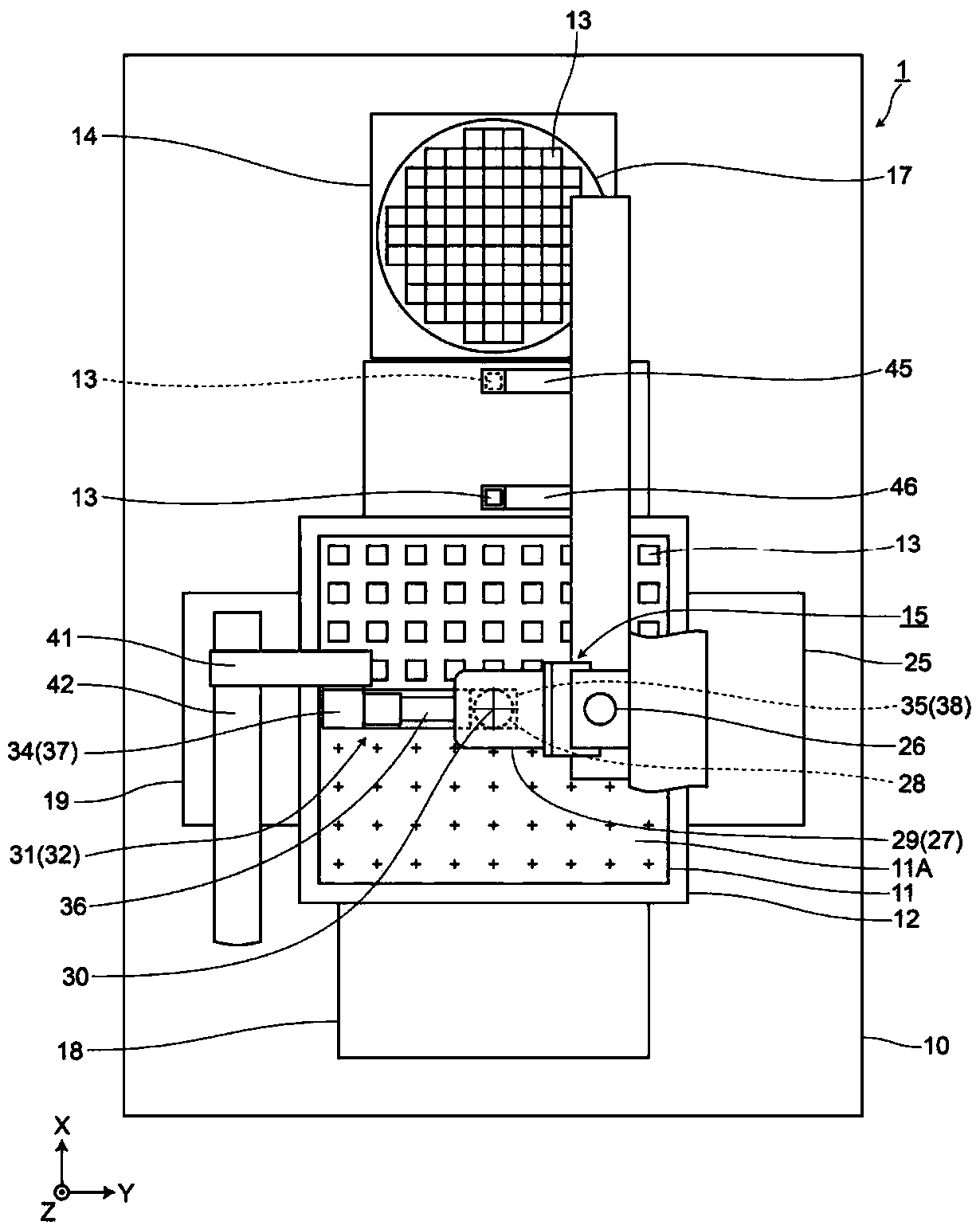
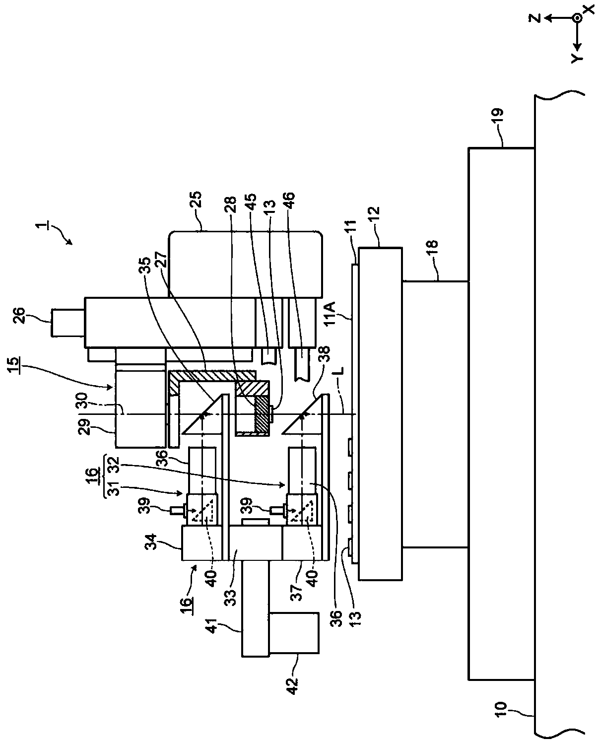
[0033] Hereinafter, for the electronic component mounting apparatus 1 and the electronic component mounting method in the embodiment of the present invention, reference will be made to Figure 1-Figure 5 Be explained.

[0034] [Structure of Electronic Component Mounting Device 1 ]

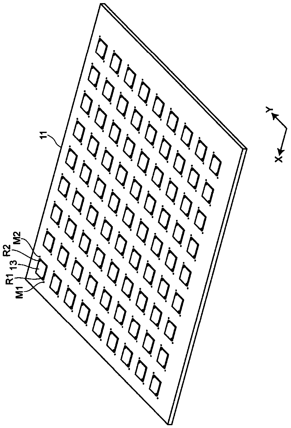
[0035] figure 1 It is a plan view showing a rough structure of the electronic component mounting apparatus 1 in the embodiment,

[0036] figure 2 is displayed from figure 1 A front view of the electronic component mounting apparatus 1 seen from the lower side of the figure. The figure described below, will figure 1 The left-right direction in the diagram is referred to as the Y direction or the Y axis, and the up-down direction in the diagram is referred to as the X direction or the X-axis. Alternatively, the vertical direction with respect to the X-Y plane will be described as the Z direction or the vertical direction.

[0037] refer to figure 1 , figure 2 Next, the structure of the ele...


PUM


Abstract

The purpose of the present invention is to provide an electronic component mounting device and an electronic component mounting method capable of accurately performing position alignment of a chip component and a substrate at a short beat time. The electronic component mounting device (1) and the electronic component mounting method according to the present invention are provided with: a chuck (28) that is formed of a transparent material and holds a chip component (13) attached thereto; a first mirror (35) that is provided on the opposite side of the chip component (13) with respect to the chuck (28) and projects an image of the chip component (13); a chip component recognition camera 34 that recognizes the chip component 13; a second mirror 38 provided between the substrate 11 and the chuck 28 and projecting an image of the substrate 11; and a substrate recognition camera 37 that recognizes the substrate 11, wherein the first mirror (35) and the second mirror (38) integrally move tothe chip component (13) and the substrate (11) at the recognition operation positions A and B, and after the positions of the chip component (13) and the substrate (11) are recognized, the position deviation of the chip component (13) and the substrate (11) is corrected on the basis of the recognition information.

Description

technical field [0001] The present invention relates to an electronic component mounting device and an electronic component mounting method. Background technique [0002] When mounting an electronic component (called a chip component) like a semiconductor chip on a substrate, the chip component and the substrate must be aligned with high precision and then bonded together. This alignment usually involves identifying the chip component identification mark provided on the chip component and the substrate identification mark provided on the substrate with a camera or the like, and controlling the relative positional relationship between the two identification marks to a specified value. accuracy. A device that mounts chip components on a substrate is called an electronic component mounting device, a die bonder, or a bonding device. [0003] As an alignment means between a chip component and a substrate, there is an electronic component mounting apparatus including: a camera f...

Claims


Application Information

Patent Timeline
Patent Type & Authority Applications(China)
IPC IPC(8): H05K13/04H05K13/08
CPCH01L21/52H01L21/67092H01L21/67121H01L21/67144H01L21/67259H01L21/682
Inventor 山岸昭隆宫坂研吾上岛直人本藤弘敏
Owner ATHLETE FA KK
Why Eureka
Try Eureka