Optical element surface defect detection method based on deep learning

A kind of defect detection and optical component technology, which is applied in the direction of image data processing, instruments, biological neural network models, etc., can solve problems such as small size, low detection efficiency, and difficult to give accurate detection results. The effect of low rate

Active Publication Date: 2019-06-25
INST OF OPTICS & ELECTRONICS - CHINESE ACAD OF SCI
View PDF20 Cites 18 Cited by
  • Summary
  • Abstract
  • Description
  • Claims
  • Application Information

AI Technical Summary

Problems solved by technology

Since the detection results of the visual method are limited by the resolution ability of the human eye and the subjective judgment of the inspector, it is difficult to give accurate detection results for defects with small size and poor contrast
In addition, some methods based on imaging, scattered energy analysis, laser spectrum analysis, and microscopic surface profiler measurement have also been used in defect detection, but they have more or less problems, such as the inability to accurately obtain the number of defects and location, detection accuracy is not high, detection efficiency is low, quantitative analysis cannot be performed, etc.

Method used


Image

  • Optical element surface defect detection method based on deep learning
  • Optical element surface defect detection method based on deep learning
  • Optical element surface defect detection method based on deep learning

Examples


Embodiment

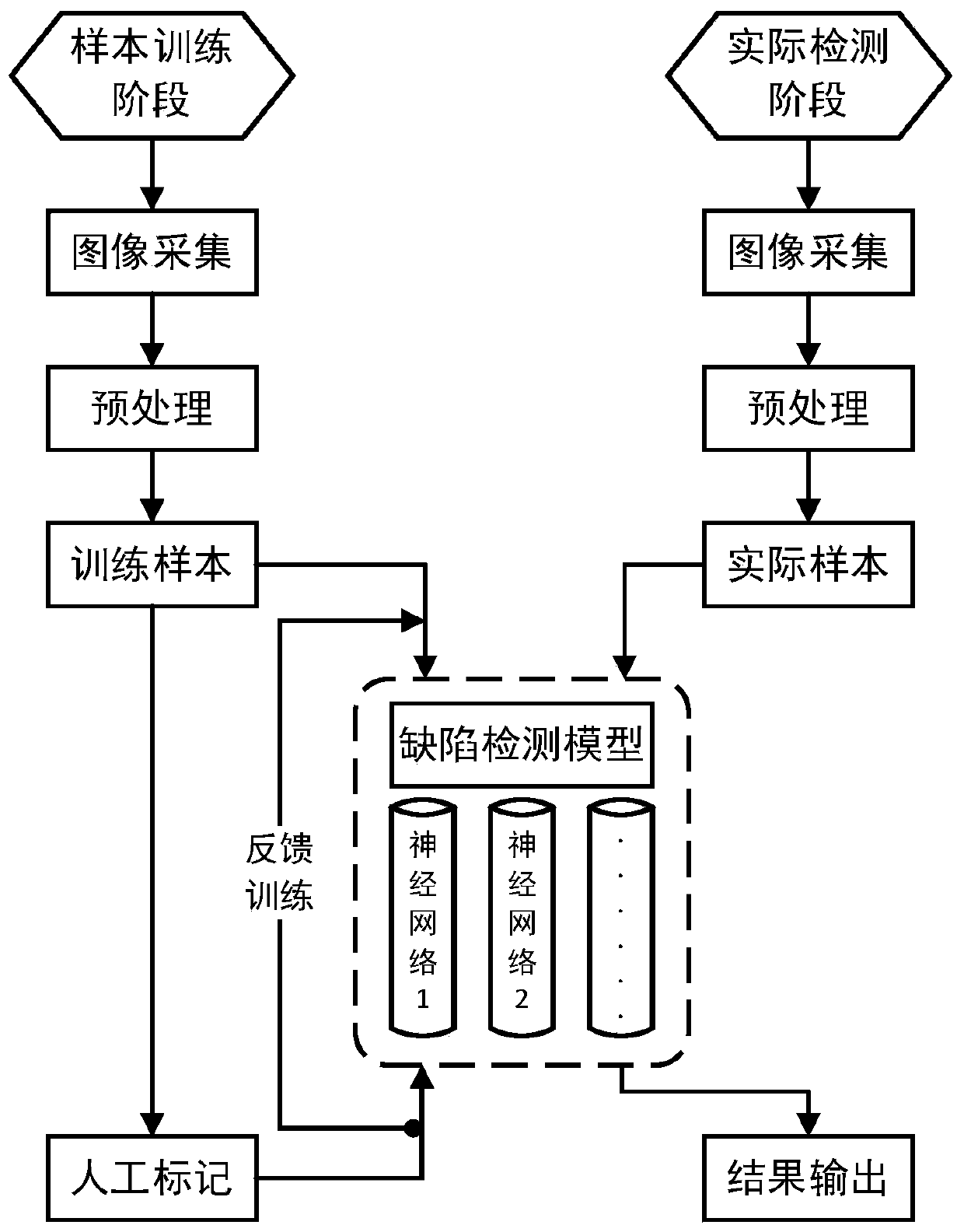
[0033] The present invention will be described in further detail below with reference to the accompanying drawings and specific embodiments. It must be pointed out that the embodiments are only used to further describe the present invention, and do not imply any limitation to the protection scope of the present invention. like figure 1 As shown, a deep learning-based optical element surface defect detection method proposed by the present invention specifically includes the following steps:

[0034] 1) Obtain and preprocess images of surface defects of optical components;

[0035] 2) Input the pre-processed defect image into the pre-trained defect detection model for intelligent identification of surface defects of optical components.

[0036] Among them, the defect detection model is a neural network based on deep learning, including sequentially cascaded feature extraction networks, classifiers, and regressors. The feature extraction network performs feature extraction on th...


PUM


Abstract

The invention discloses an optical element surface defect detection method based on deep learning. The method comprises the following steps: 1) obtaining and preprocessing an optical element surface defect image; and 2) inputting the preprocessed defect image into a pre-trained defect detection model to carry out intelligent identification on the surface defects of the optical element. In the image preprocessing step, distortion correction is carried out on a collected image, and the image is processed by adopting a gradient image adaptive threshold segmentation method, an edge detection method, binarization processing and breakpoint connection algorithm fusion mode. The defect detection model is a multi-layer neural network model composed of a convolution layer, a pooling layer, a full connection layer and the like. Compared with the prior art, the method has the advantages that the problems of subjective interference, difficulty in accurate quantification and the like caused by manual visual detection are solved, and the problems of low accuracy, high omission factor and the like of an imaging detection method in a defect recognition process are solved.

Description

technical field [0001] The invention belongs to the field of surface defect detection of optical elements, and in particular relates to a method for detecting surface defects of optical elements based on deep learning. Background technique [0002] With the continuous development of advanced optical manufacturing technology, application fields such as microelectronics equipment, aerospace, precision measurement and laser systems have put forward higher technical requirements for the surface processing quality of precision optical components, which are their core components. Especially in some high-precision optical systems, there are strict control requirements on the surface defects of optical components. However, due to the existence of various uncertain factors, surface defects cannot be completely avoided even with modern precision machining technology. Surface defects are one of the important evaluation indicators for evaluating the processing quality of optical compon...

Claims


Application Information

Patent Timeline
Patent Type & Authority Applications(China)
IPC IPC(8): G06T7/00G06N3/04
Inventor 胡小川全海洋徐富超付韬韬侯溪李声
Owner INST OF OPTICS & ELECTRONICS - CHINESE ACAD OF SCI
Why Eureka
Try Eureka