Display panel and display device
A display panel and display device technology, which is applied in semiconductor devices, electrical components, circuits, etc., can solve problems such as shape change, abnormal overlap, and influence on cathode stability, so as to improve stability, prevent deformation or damage, The effect of prolonging life
- Summary
- Abstract
- Description
- Claims
- Application Information
AI Technical Summary
Problems solved by technology
Method used
Image


Examples
Embodiment Construction
[0026] In order to make the purpose, technical solution and effect of the present application more clear and definite, the present application will be further described in detail below with reference to the accompanying drawings and examples.
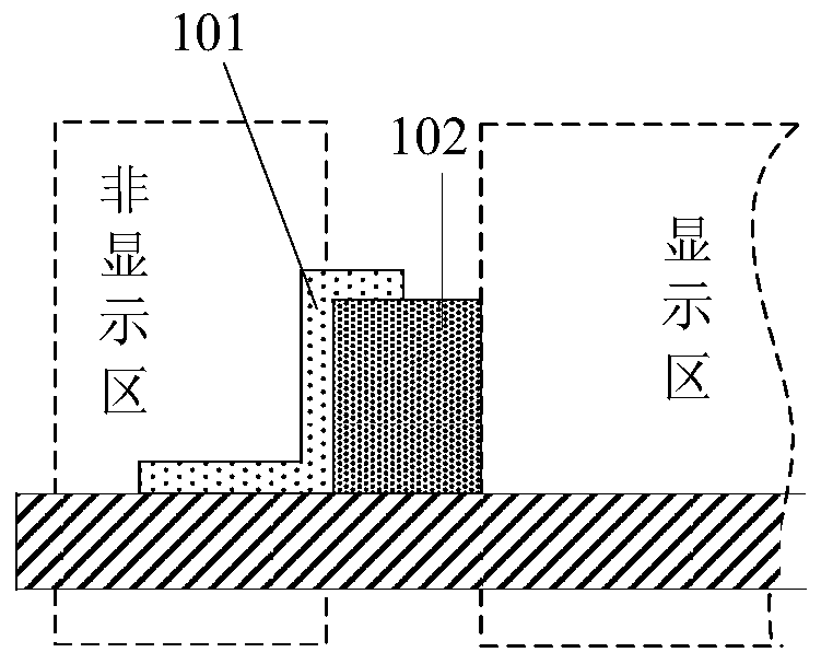
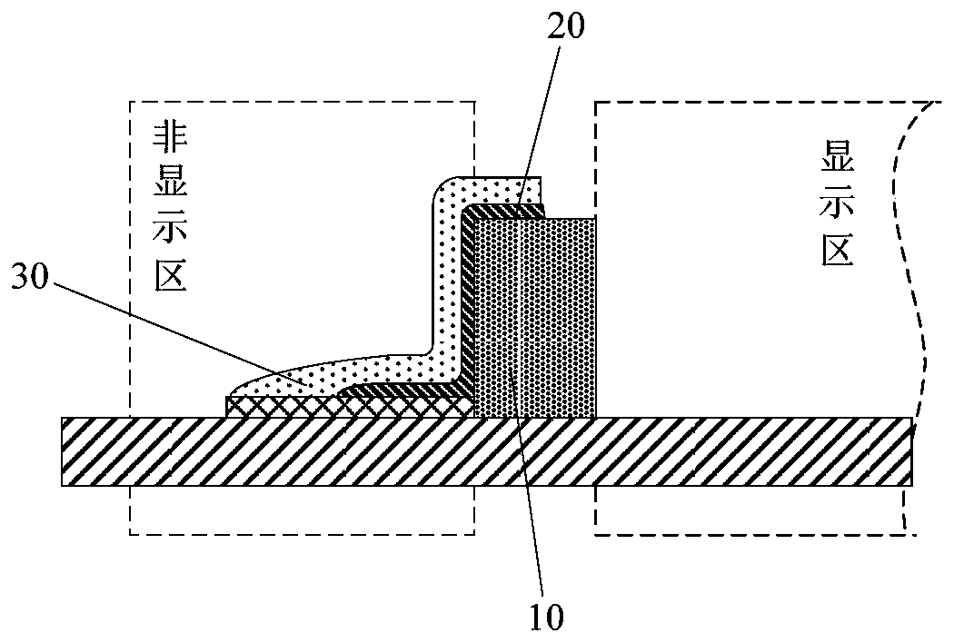
[0027] The application provides a display panel, the display panel includes a display area and a non-display area outside the display area, a boundary layer separating the display area from the non-display area, a flat layer in the non-display area, the flat layer at least covers the boundary The boundary area between the layer and the non-display area, the electrode layer, the electrode layer covers at least the non-display area and the boundary layer. By setting the flat layer so that it covers the boundary area between the defining layer and the non-display area, the flat layer can be used to form a buffer between the electrode layer and the defining layer, reducing the difficulty of climbing the electrode when forming the electrode, ...
PUM
 Abstract
Description
Claims
Application Information
 - R&D
- Intellectual Property
- Life Sciences
- Materials
- Tech Scout
- Unparalleled Data Quality
- Higher Quality Content
- 60% Fewer Hallucinations
Browse by: Latest US Patents, China's latest patents, Technical Efficacy Thesaurus, Application Domain, Technology Topic, Popular Technical Reports.
© 2025 PatSnap. All rights reserved.Legal|Privacy policy|Modern Slavery Act Transparency Statement|Sitemap|About US| Contact US: help@patsnap.com