Supercharge Your Innovation With Domain-Expert AI Agents!

Chip scale package structures

A wafer-level chip and size packaging technology, which is applied to semiconductor/solid-state device components, semiconductor devices, electrical components, etc., can solve the problem of rising overall chip costs

Active Publication Date: 2019-07-05
IND TECH RES INST
View PDF6 Cites 0 Cited by
  • Summary
  • Abstract
  • Description
  • Claims
  • Application Information

AI Technical Summary

Problems solved by technology

However, this technology still has its bottleneck. To achieve chip-to-chip bonding assembly technology, for now, it can only be applied to small sensors
The reason is that although the chip pitch of the memory chip / logic chip can be adjusted to match the pitch of the image sensor as much as possible, however, when the area of ​​the sensor continues to increase, the chip pitch of the memory chip / logic chip will inevitably increase accordingly. At this time, the number of memory chips / logic chips per unit wafer area will decrease, resulting in a significant increase in overall wafer cost

Method used


Image

  • Chip scale package structures
  • Chip scale package structures
  • Chip scale package structures

Examples


Embodiment Construction

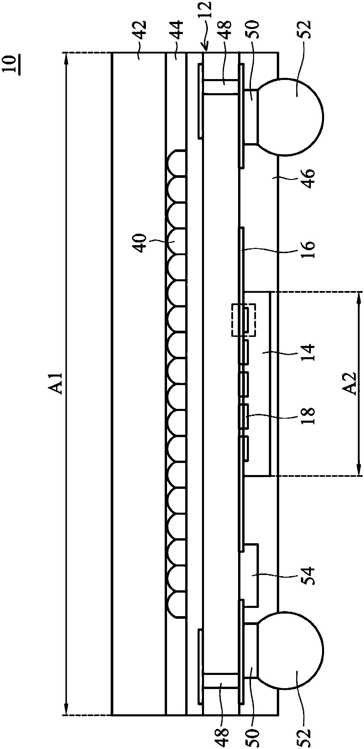
[0056] See figure 1 According to an embodiment of the present invention, a wafer level chip scale package (WLCSP) structure 10 is disclosed. figure 1 It is a schematic cross-sectional view of a wafer level chip scale package (WLCSP) structure 10.

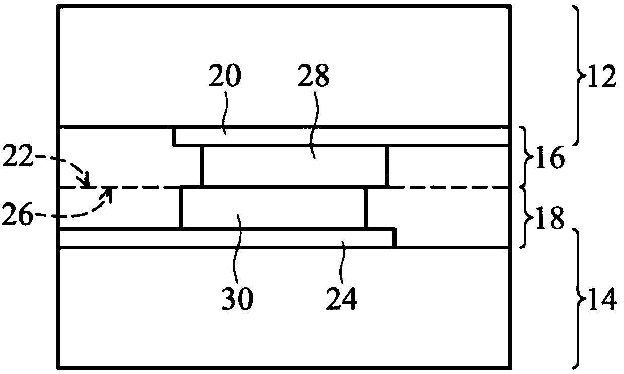
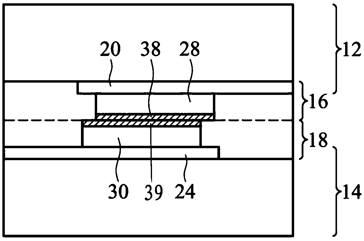
[0057] In this embodiment, the wafer level chip scale package (WLCSP) structure 10 includes an image sensor chip 12 and a chip 14. The image sensor chip 12 includes a first redistribution layer 16. The chip 14 includes a second redistribution layer 18. The area A2 of the chip 14 is smaller than the area A1 of the image sensor chip 12. The internal structure of the first redistribution layer 16 and the second redistribution layer 18 and the bonding state between the image sensor chip 12 and the chip 14 (in the dotted frame in the figure) will be described in detail later.

[0058] In some embodiments, the image sensor chip 12 can also be replaced by other sensor chips, such as an acoustic wave sensor chip, a temperature sensor chip, a h...


PUM


Abstract

The present invention discloses a chip scale package structure. The chip scale package structure includes an image sensor chip and a chip. The image sensor chip includes a first redistribution layer including a conductive wire and a conductive pad formed on the conductive wire, wherein the conductive pad is exposed from the surface of the first redistribution layer. The chip includes a second redistribution layer including a conductive wire and a conductive pad formed on the conductive wire, wherein the conductive pad is exposed from the surface of the second redistribution layer. The area ofthe chip is smaller than that of the image sensor chip. The second redistribution layer of the chip bonds the first redistribution layer of the image sensor chip.

Description

Technical field [0001] The invention relates to a wafer level chip size package (WLCSP) structure. Background technique [0002] The packaging manufacturing process of the traditional image sensor module is based on wire-bonding packaging or chip-scale packaging (CSP). For the overall image sensor module system, the memory chip and control chip are still needed for data access and control. Therefore, the image sensor, memory chip and control chip are usually assembled and integrated on the system board. The communication between the memory chip, the control chip and the image sensor is carried out through this system board. [0003] Recently, due to the innovation in the manufacturing process of image sensors and the substantial increase in pixels, the demand for huge amounts of data access and control has increased. For traditional system integration methods, it is not enough to deal with market trends. Therefore, some companies have developed an assembly technology that integr...

Claims


Application Information

Patent Timeline
Patent Type & Authority Applications(China)
IPC IPC(8): H01L23/31H01L23/485
CPCH01L23/31H01L23/485H01L27/14625H01L27/14618H01L27/14627H01L23/3114H01L2224/80895H01L2224/80357H01L2224/05582H01L2224/05644H01L2224/05657H01L2224/05611H01L2224/05649H01L2224/05666H01L2224/05664H01L2224/05655H01L2224/05639H01L2224/80896H01L2224/08145H01L2224/0401H01L2224/0603H01L2224/091H01L2224/05647H01L2224/16145H01L2224/13082H01L24/08H01L24/05H01L24/09H01L24/17H01L24/16H01L24/13H01L2224/05008H01L2224/05569H01L2224/131H01L2224/13147H01L2924/00014H01L2924/014H01L27/14632H01L2224/02373H01L24/73H01L23/3128H01L24/29
Inventor 林育民张道智
Owner IND TECH RES INST
Features
  • R&D
  • Intellectual Property
  • Life Sciences
  • Materials
  • Tech Scout
  • Unparalleled Data Quality
  • Higher Quality Content
  • 60% Fewer Hallucinations
Learn More