Pixel definition layer and preparation method thereof, and display substrate and display device comprising same
A technology of pixel-defining layer and pixel area, applied in electrical components, electric solid-state devices, circuits, etc., can solve problems such as failure and short performance retention time, improve the hydrophilic/hydrophobic performance, and improve equipment utilization and production capacity. Effect
- Summary
- Abstract
- Description
- Claims
- Application Information
AI Technical Summary
Problems solved by technology
Method used
Image


Examples
Embodiment Construction
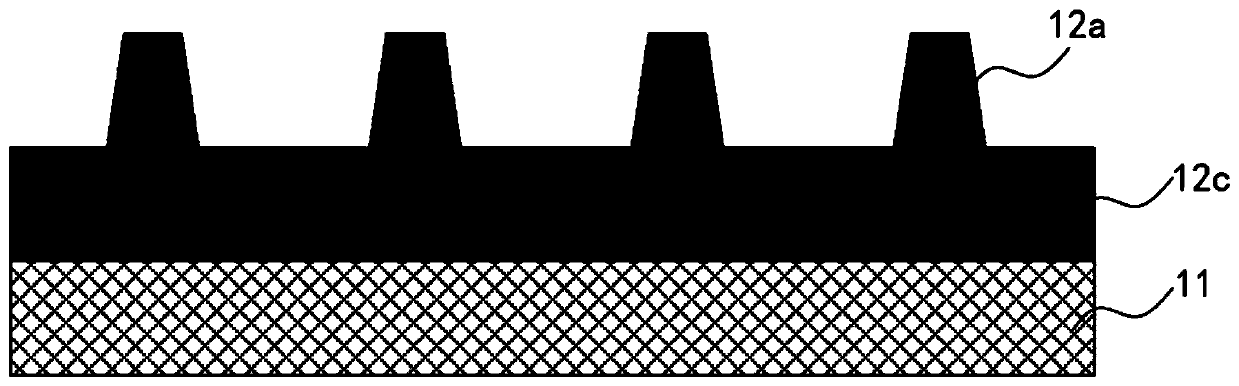
[0034] Example embodiments will now be described more fully with reference to the accompanying drawings. Example embodiments, however, can be embodied in various forms and should not be construed as limited to the embodiments set forth herein; rather, these embodiments are provided so that this disclosure will be thorough and complete, and will fully convey the concept of example embodiments to those skilled in the art. In the drawings, the thickness of regions and layers are exaggerated for clarity. The same reference numerals in the drawings denote the same or similar structures, and thus their detailed descriptions will be omitted.
[0035] It should be noted that the terms upper and lower in the present invention are only relative concepts to each other or refer to the normal use state of the product, and should not be regarded as limiting. For the same reason, the terms first, second, etc., are only used to distinguish descriptions, and should not be construed as indica...
PUM
 Abstract
Description
Claims
Application Information