A multi-layer stacked vertically interconnected radio frequency structure and its manufacturing method

A manufacturing method and stacking technology, applied in semiconductor/solid-state device manufacturing, circuits, electrical solid-state devices, etc., can solve problems such as area reduction and difficulty in heat dissipation of upper-layer chips, and achieve the effect of solving insufficient antenna area

Active Publication Date: 2021-02-09
GREAT MICROWAVE TECH CO LTD
View PDF5 Cites 0 Cited by
  • Summary
  • Abstract
  • Description
  • Claims
  • Application Information

AI Technical Summary

Problems solved by technology

However, for analog device chips such as radio frequency chips, the area cannot be reduced exponentially like digital chips. In this way, there will be no enough area for ultra-high frequency radio frequency microsystems to place PA / LNA at the same time. LNAs are stacked, so it will become very difficult to dissipate heat from the upper chip based on the heat-conducting copper pillars

Method used


Image

  • A multi-layer stacked vertically interconnected radio frequency structure and its manufacturing method
  • A multi-layer stacked vertically interconnected radio frequency structure and its manufacturing method
  • A multi-layer stacked vertically interconnected radio frequency structure and its manufacturing method

Examples


Embodiment Construction

[0033] Embodiments of the present invention are described in detail below, wherein the same or similar reference numerals represent the same or similar elements or elements with similar functions. The embodiments described below by referring to the figures are exemplary, and are only used to explain the present invention and not to limit the present invention.

[0034] Those skilled in the art can understand that, unless otherwise defined, all terms (including technical terms and scientific terms) used herein have the same meanings as commonly understood by those of ordinary skill in the art to which this invention belongs. It should also be understood that terms such as those defined in commonly used dictionaries should be understood to have a meaning consistent with the meaning in the context of the prior art, and unless defined as herein, will not be used in an idealized or overly formal meaning to explain.

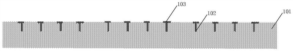
[0035] The reference numerals related to the steps mentioned in ...


PUM


Abstract

The invention discloses a multi-layer stacked vertically interconnected radio frequency structure, which includes an antenna array element, a heat dissipation carrier board, a base carrier board and a radio frequency module. The antenna array element is mounted on the upper surface of the heat dissipation carrier board and the lower surface of the heat dissipation carrier board It is welded with the upper surface of the base carrier plate, and the RF module is mounted on the lower surface of the base carrier plate; wherein, the lower surface of the heat dissipation carrier plate is provided with a flow port horizontally, one side of the flow port extends to the side of the heat dissipation carrier plate, and the heat dissipation carrier plate is vertically arranged with multiple rows Through metal columns, metal columns are set at corresponding positions on the base carrier plate, and through holes are set between the metal columns on the base carrier plate; A radio frequency structure of layer-stacked vertical interconnection and a manufacturing method thereof.

Description

technical field [0001] The invention relates to the technical field of semiconductors, more specifically, it relates to a multi-layer stacked vertically interconnected radio frequency structure and a manufacturing method thereof. Background technique [0002] Microwave and millimeter wave radio frequency integrated circuit technology is the foundation of modern national defense weaponry and Internet industry. Millimeter-wave radio frequency integrated circuits also have huge actual needs and potential markets. [0003] However, for high-frequency microsystems, the area of ​​the antenna array is getting smaller and smaller, and the distance between the antennas must be kept within a certain range so that the entire module can have excellent communication capabilities. However, for analog device chips such as radio frequency chips, the area cannot be reduced exponentially like digital chips. In this way, there will be no enough area for ultra-high frequency radio frequency mi...

Claims


Application Information

Patent Timeline
Patent Type & Authority Patents(China)
IPC IPC(8): H01L23/473H01L23/367H01L21/48H01Q1/22H01Q21/00
CPCH01L21/4871H01L21/4882H01L23/3675H01L23/473H01Q1/2283H01Q21/00
Inventor 张兵张勋宋启河
Owner GREAT MICROWAVE TECH CO LTD
Why Eureka
Try Eureka