Micro LED chip structure, manufacturing method thereof and display panel

A technology of LED chip and manufacturing method, which is applied in the direction of electrical components, electric solid devices, circuits, etc., and can solve the problems of micro-LED chip fragmentation and the like

Inactive Publication Date: 2021-08-13
苏州芯聚半导体有限公司
View PDF4 Cites 0 Cited by
  • Summary
  • Abstract
  • Description
  • Claims
  • Application Information

AI Technical Summary

Problems solved by technology

[0004] The present invention provides a micro-LED chip structure, manufacturing method and display panel, which overcomes the problem of micro-LED chip fragmentation during the pressing and binding process of the existing micro-LED chip and the driving backplane

Method used


Image

  • Micro LED chip structure, manufacturing method thereof and display panel
  • Micro LED chip structure, manufacturing method thereof and display panel
  • Micro LED chip structure, manufacturing method thereof and display panel

Examples


Embodiment Construction

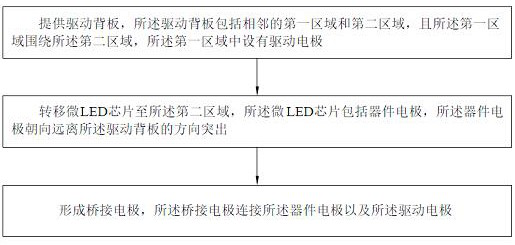
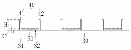
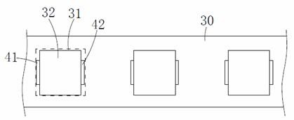
[0044] In order to make the object, technical solution and advantages of the present invention clearer, the present invention will be further described in detail below in conjunction with the embodiments and accompanying drawings. It should be understood that the specific embodiments described here are only used to explain the present invention, not to limit the present invention.

[0045] In the description of the present invention, it should be noted that the terms "center", "upper", "lower", "left", "right", "vertical", "horizontal", "inner", "outer" etc. The indicated orientation or positional relationship is based on the orientation or positional relationship shown in the drawings, and is only for the convenience of describing the present invention and simplifying the description, rather than indicating or implying that the referred device or element must have a specific orientation, or in a specific orientation. construction and operation, therefore, should not be constr...


PUM

PropertyMeasurementUnit
thicknessaaaaaaaaaa

Abstract

The invention provides a micro LED chip structure, a manufacturing method thereof and a display panel. The manufacturing method comprises the following steps: providing a driving backboard, wherein the driving backboard comprises a first region and a second region which are adjacent, the first region surrounds the second region, and the first region is provided with a driving electrode; transferring a micro LED chip to the second region, wherein the micro LED chip comprises a device electrode, and the device electrode protrudes in the direction away from the driving backboard; and forming a bridging electrode, wherein the bridging electrode is connected with the device electrode and the driving electrode.

Description

technical field [0001] The invention belongs to the technical field of manufacturing semiconductor devices, and in particular relates to a micro LED chip, a manufacturing method and a display panel. Background technique [0002] In recent years, semiconductor micro-LED chips have developed rapidly as an active light-emitting micro-display technology. The application scenarios of micro-LED chip display technology cover all display ranges, such as large commercial display screens, TVs, mobile phones, vehicle displays, AR and VR, etc. In particular, the micro-LED chip display technology used in micro-displays such as AR and VR has incomparable advantages over other display technologies, such as high brightness and high pixel density. [0003] At present, the relevant technologies for the application of micro-LED chips in the production of display panels are still immature, and the production schemes are based on different mass transfer methods and repair methods. The micro LED...

Claims


Application Information

Patent Timeline
Patent Type & Authority Applications(China)
IPC IPC(8): H01L33/00H01L33/62H01L27/15
CPCH01L27/156H01L33/0095H01L33/62
Inventor 李庆于波韦冬
Owner 苏州芯聚半导体有限公司
Why Eureka
Try Eureka