Wafer-level packaging structure and wafer-level packaging method

A technology of wafer-level packaging and packaging methods, which is applied in the direction of electrical components, electric solid-state devices, circuits, etc., can solve the problems of high technical difficulty, high cost of wafer-level packaging, and low space utilization, and achieve low technical difficulty, Avoid packaging technology, the effect of efficient use of space

Pending Publication Date: 2020-03-17
NAT CENT FOR ADVANCED PACKAGING
View PDF0 Cites 0 Cited by
  • Summary
  • Abstract
  • Description
  • Claims
  • Application Information

AI Technical Summary

Problems solved by technology

[0004] Therefore, the technical problem to be solved by the present invention is to overcome the defects of high wafer-level packaging cost, high technical difficulty, and low space utilization rate in the prior art, so as to provide a wafer-level packaging structure and packaging method

Method used


Image

  • Wafer-level packaging structure and wafer-level packaging method
  • Wafer-level packaging structure and wafer-level packaging method
  • Wafer-level packaging structure and wafer-level packaging method

Examples


Embodiment 1

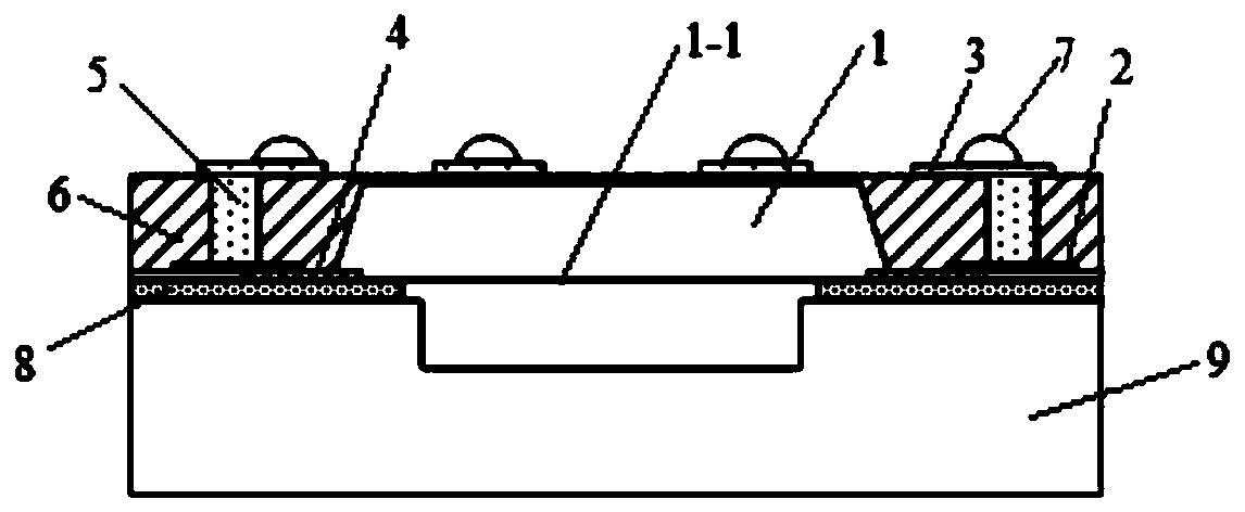
[0041] This embodiment provides a wafer-level packaging structure, see figure 1 , comprising, a plastic encapsulation layer 6, a first wafer 1, a carrier 9, a conductive metal pillar 5, a first redistribution layer 2 and a second redistribution layer 3;

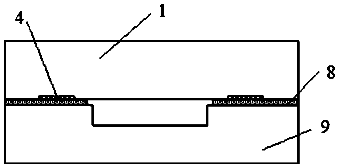
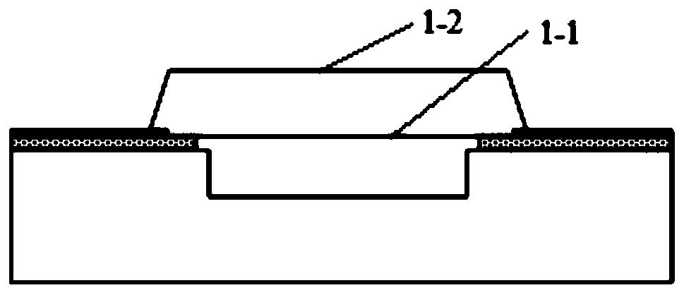
[0042] The first wafer 1 is covered in the plastic encapsulation layer 6, the front surface 1-1 of the first wafer is arranged opposite to the carrier, the carrier is bonded to the front of the first wafer through the bonding layer 8, and there is a groove in the carrier , the groove is arranged opposite to the front surface 1-1 of the first wafer; the conductive metal pillar 5 is arranged through the plastic sealing layer 6, and the first end of the conductive metal pillar is arranged in the plastic sealing layer, and the second end is exposed on one side of the plastic sealing layer; The first redistribution layer 2 is electrically connected to the first end 5-1 of the conductive metal pillar 5 and the front surface of the ...

Embodiment 2

[0046] This embodiment provides an improved scheme for wafer-level packaging structure, see figure 1, comprising, a plastic encapsulation layer 6, a first wafer 1, a carrier 9, a conductive metal pillar 5, a first redistribution layer 2, a second redistribution layer 3, a first pad 4 and a second pad 7;

[0047] The first wafer 1 is covered in the plastic encapsulation layer 6, the front surface 1-1 of the first wafer is arranged opposite to the carrier, the carrier is bonded to the front of the first wafer through the bonding layer 8, and there is a groove in the carrier , the groove is arranged opposite to the front of the first wafer; the conductive metal post 5 is arranged through the plastic encapsulation layer 6, and the first end of the conductive metal post is arranged in the plastic encapsulation layer, and the second end is exposed on the side of the plastic encapsulation layer; the first heavy The wiring layer 2 is electrically connected to the first end 5-1 of the ...

Embodiment 3

[0051] This embodiment provides a packaging method for a wafer-level packaging structure, the flow chart of which is shown in Figure 2A-Figure 2F , including the following steps,

[0052] The first wafer 1 is flip-chip setup, with the front side 1-1 facing down, see Figure 2A , the front of the first wafer is bonded to the carrier 9 through the bonding layer 8, and after mechanical cutting, the back of the first wafer is grooved to form an opening, see Figure 2B , exposing part of the first pad 4;

[0053] The opening is redistributed to form the first redistribution layer 2, see Figure 2C , the top view rendering of the first rewiring layer is shown in image 3 ;

[0054] Through the electroplating process, conductive metal pillars 5 are formed on the first rewiring layer 2, and the plastic sealing layer 6 is formed after filling with glue, see Figure 2D , and then thinning the plastic encapsulation layer, so that the second end 5-2 of the conductive metal post is e...


PUM


Abstract

The invention belongs to the technical field of packaging, and particularly relates to a wafer-level packaging structure and a wafer-level packaging method. The wafer-level packaging structure comprises a plastic packaging layer, a first wafer, a conductive metal column, a rewiring layer and a slide glass, according to the structure, the conductive metal columns are arranged in the plastic packaging layer; wherein the two ends of the first wafer are electrically connected with the rewiring layer respectively, the front surface of the first wafer is electrically connected with the first rewiring layer, and the second rewiring layer is arranged in the direction of the back surface of the first wafer, so that the wafer-level packaging structure can realize back surface electric interconnection without a TSV process, and the space utilization rate can be improved by arranging the first rewiring layer; in practical application, the first rewiring layer can realize direct interconnection ofthe first wafers, the space utilization rate is improved, the layout of the second rewiring layer is facilitated, and the application of the first rewiring layer is wider.

Description

technical field [0001] The invention belongs to the technical field of packaging, and in particular relates to a wafer-level packaging structure and packaging method. Background technique [0002] Wafer-level packaging (WLP) is a type of IC packaging. As an advanced packaging technology, all process steps are completed before the wafer is sliced. Wafer-level chip-scale packaging is a combination of wafer-level packaging and chip-scale packaging. After the front-end process of the wafer is completed, the wafer is directly packaged at the wafer level, and the interconnection bumps are performed on the wafer. Point and test. [0003] Wafer-level packaging has achieved rapid growth in MEMS and CIS (CMOS image sensors) due to its advantages of high packaging processing efficiency, small and thin package size, and good electrothermal performance. The interconnection wires in the package usually do not need wire bonding. There are three common ways, the first is to directly make ...

Claims


Application Information

Patent Timeline
Patent Type & Authority Applications(China)
IPC IPC(8): H01L23/31H01L23/538H01L21/48
CPCH01L21/4814H01L23/3114H01L23/315H01L23/5386H01L2224/11
Inventor 任玉龙曹立强
Owner NAT CENT FOR ADVANCED PACKAGING
Why Eureka
Try Eureka