Unlock instant, AI-driven research and patent intelligence for your innovation.

Compensation circuit for compensating input bias voltage of error amplifier

An error amplifier and compensation circuit technology, which is applied to differential amplifiers, amplifiers, and components of amplifying devices, etc., can solve problems such as difficulty in knowing offset current and difficulty in transistor design.

Active Publication Date: 2019-07-19
ELITE SEMICON MEMORY TECH INC
View PDF11 Cites 0 Cited by
  • Summary
  • Abstract
  • Description
  • Claims
  • Application Information

AI Technical Summary

Problems solved by technology

Unfortunately, the variation of offset current with process variation is not easy to know, nor is it easy to design for matching more than two transistors

Method used


Image

  • Compensation circuit for compensating input bias voltage of error amplifier
  • Compensation circuit for compensating input bias voltage of error amplifier
  • Compensation circuit for compensating input bias voltage of error amplifier

Examples


Embodiment Construction

[0060] Reference will now be made in detail to the exemplary embodiments of the invention, which are illustrated in the accompanying drawings. Wherever possible, the same reference numbers will be used in the drawings and description to refer to the same or like parts.

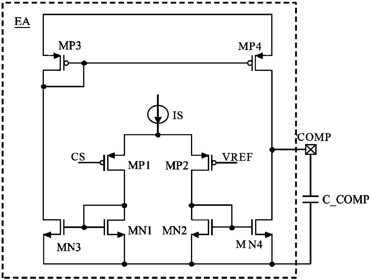
[0061] Exemplary embodiments of the present invention provide a compensation circuit used in an error amplifier circuit, and the compensation circuit may compensate an input bias voltage of an error amplifier in the error amplifier circuit. The compensation circuit compensates for the input bias voltage ahead of the input of the error amplifier, so that only the input bias voltage needs to be measured during circuit probing. Then, a trim code for the input bias voltage can be calculated, where the trim code records the ratio relationship between the input bias voltage and the resistor value to be trimmed.

[0062] In an exemplary embodiment of the present invention, resistors should be designed to match each ...


PUM


Abstract

A compensation circuit for compensating an input bias of an error amplifier has a level shifter, a first trimming circuit, a second trimming circuit, and a compensation current absorbing device. The level shifter moves the level of the feedback voltage and the level of the predetermined reference voltage and outputs a level shift feedback voltage and a level shift reference voltage. The first trimming circuit trims its first resistance value according to a trimming code having a ratio relationship between an input bias voltage and a resistance value to be trimmed to adjust a level shift reference voltage. The second trimming circuit adjusts the level shift feedback voltage according to the trimming code. The compensation current absorbing device absorbs the current passing through the first trimming circuit and the current passing through the second trimming circuit.

Description

technical field [0001] The present invention relates to an error amplifier circuit, and in particular to a compensation circuit for compensating an input bias voltage of an error amplifier and an error amplifier circuit having the compensation circuit. Background technique [0002] Switching light-emitting diode (LED) drivers currently on the market operate in boundary current mode (BCM) and also have a dead-loop circuit for locking the LED current. refer to Figure 1A , Figure 1A is a schematic diagram of a conventional switch-mode LED driver. A conventional switch-mode LED driver 1 includes a current-voltage converter 11, an error amplifier EA, a compensation capacitor C_COMP and a comparator CMP. The current-voltage converter 11 is connected to the error amplifier EA, which is connected to the compensation capacitor C_COMP and the comparator CMP. [0003] The LED current iLED (ie, the current through the LED) is fed back to the switch mode LED driver 1, and the current...

Claims


Application Information

Patent Timeline
IPC IPC(8): H03F1/30H03F3/45H05B33/08H05B44/00
CPCH03F1/301H03F3/45273H05B45/37H05B45/10Y02B20/30
Inventor 何仪修
Owner ELITE SEMICON MEMORY TECH INC
Features
  • R&D
  • Intellectual Property
  • Life Sciences
  • Materials
  • Tech Scout
  • Unparalleled Data Quality
  • Higher Quality Content
  • 60% Fewer Hallucinations
Learn More