Printing quality detection method of PCB board labeling based on deep learning

A PCB board and deep learning technology, applied in image analysis, image enhancement, instruments, etc., can solve the problems of low manual detection efficiency, high detection cost, and inability to effectively guarantee detection accuracy, and achieve anti-background interference and anti-light conditions Strong ability, high recognition accuracy, and the effect of avoiding adverse effects

Active Publication Date: 2022-04-19
GUILIN UNIV OF ELECTRONIC TECH
View PDF5 Cites 0 Cited by
  • Summary
  • Abstract
  • Description
  • Claims
  • Application Information

AI Technical Summary

Problems solved by technology

As the demand for PCB boards continues to increase, PCB boards are developing towards high-precision and miniaturized models. The disadvantages of traditional marking and printing inspection methods are becoming more and more obvious. The efficiency of manual inspection is very low, and the inspection quality is also affected by human interference and environmental interference Due to the influence of various factors, the detection cost is too high, and the detection accuracy cannot be effectively guaranteed.

Method used


Image

  • Printing quality detection method of PCB board labeling based on deep learning
  • Printing quality detection method of PCB board labeling based on deep learning
  • Printing quality detection method of PCB board labeling based on deep learning

Examples


Embodiment

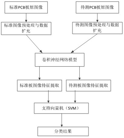
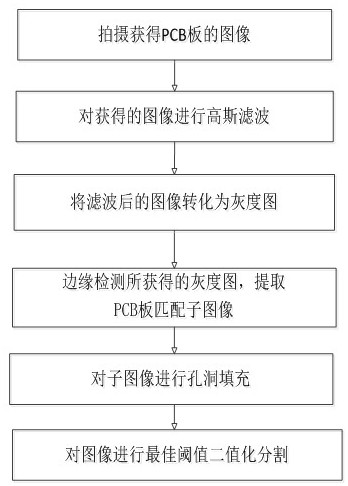
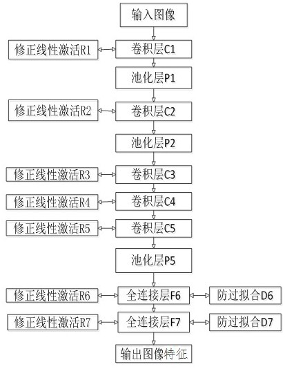
[0027] refer to Figure 1-3 , a method for detecting the printing quality of printed circuit board labels based on deep learning, including the following steps:

[0028] (1) Preprocessing the standard PCB board image: the specific sub-steps are as follows:

[0029] Step 1.1), select the PCB board without silk screen defects as the standard PCB board, use the color camera to capture the standard PCB board image, and perform Gaussian filtering on the standard PCB board image to obtain the filtered image;

[0030] Step 1.2), converting the filtered image into a grayscale image to obtain a filtered grayscale image;

[0031] Step 1.3), obtain the boundary of the PCB board matching area in the grayscale image through edge detection, and obtain the PCB board matching sub-image from the filtered image according to the boundary;

[0032] Step 1.4), use the hole filling algorithm to fill the image of the pad and other interference information data;

[0033] Step 1.5), use the Otsu al...


PUM


Abstract

The method for detecting the printing quality of PCB board marking based on deep learning in the present invention performs Gaussian filtering on the original image of the obtained PCB board, converts it into a grayscale image, edge detection, hole filling, optimal threshold value binarization and segmentation, and a series of preprocessing. It can effectively improve the identification and detection efficiency; use the Otsu algorithm to segment the image with the best threshold value to obtain a binary image, which improves the test accuracy of the present invention; effectively collect and expand the image sample data, increase the representativeness of the sample, and prevent The lack of data leads to the phenomenon of model over-fitting, so that the trained model is affected by irrelevant factors as little as possible, which enhances the robustness of the model, shortens the training time of the deep learning network, and accelerates the convergence speed; through the deep neural network The network efficiently extracts target features from images, which can effectively avoid the defects of easy overfitting, long training time, and difficult parameter adjustment caused by traditional artificial neural network feature extraction methods.

Description

technical field [0001] The invention relates to the technical field of image detection, in particular to a deep learning-based method for detecting the printing quality of PCB marking. Background technique [0002] With the rapid development of electronic information technology, PCB board, as the cornerstone of information technology, plays an increasingly important role and tends to develop in high density. In the production process of PCB boards, in order to provide users with clear instructions, it is necessary to print corresponding logo patterns and text codes on the upper and lower surfaces of the PCB board, such as component labels and nominal values, component outline shapes and manufacturer logos. , production date, etc. The process uses screen printing process, also known as screen printing process. The silk screen layer of the PCB board is the text layer, and its function is to facilitate the installation and maintenance of the circuit. In the process of markin...

Claims


Application Information

Patent Timeline
Patent Type & Authority Patents(China)
IPC IPC(8): G06T7/00G06T7/13G06T7/136G06N3/04
CPCG06T7/001G06T7/13G06T7/136G06T2207/10024G06T2207/20081G06T2207/30141G06N3/045
Inventor 李春泉陈雅琼黄红艳张明尚玉玲黄健王侨柳皓凯郝子宁刘羽佳
Owner GUILIN UNIV OF ELECTRONIC TECH
Why Eureka
Try Eureka