3d NAND flash memory and its preparation method
A flash memory and suppression layer technology, applied in semiconductor devices, electrical components, circuits, etc., can solve the problems of dielectric layer breakdown between adjacent gate layers, threshold voltage drift of gate layers, leakage of adjacent gate layers, etc. , to achieve the effect of reducing threshold voltage drift, reducing leakage, and reducing coupling effects
- Summary
- Abstract
- Description
- Claims
- Application Information
AI Technical Summary
Problems solved by technology
Method used
Image
Examples
Embodiment 1
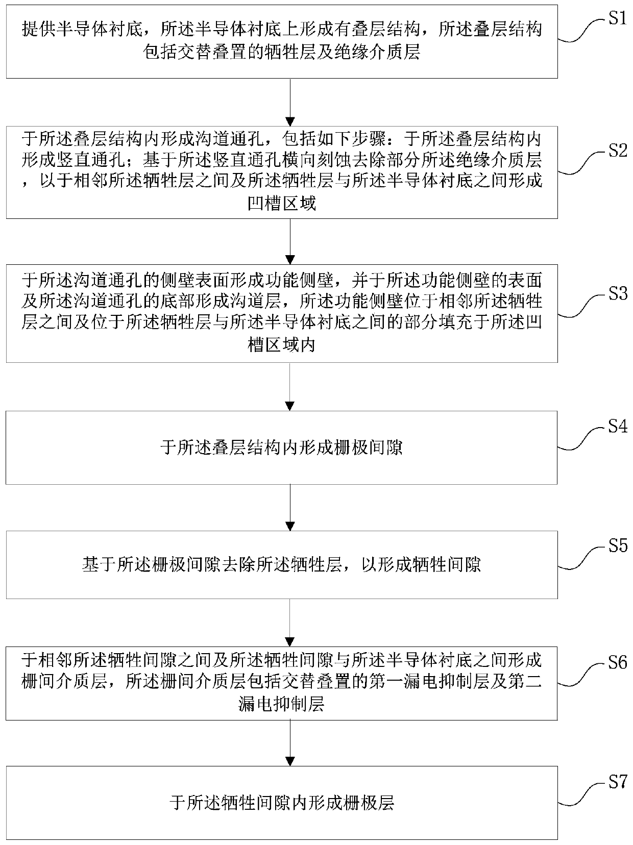
[0108] see figure 1 , the present invention provides a kind of preparation method of 3D NAND flash memory, the preparation method of described 3D NAND flash memory comprises steps:
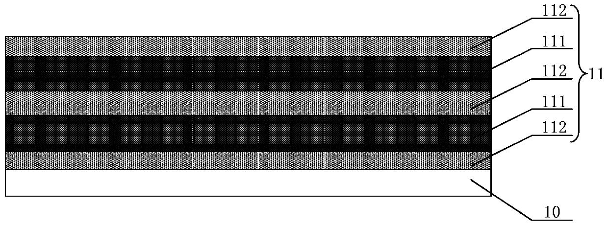
[0109] 1) providing a semiconductor substrate, on which a stacked structure is formed, and the stacked structure includes alternately stacked sacrificial layers and insulating dielectric layers;
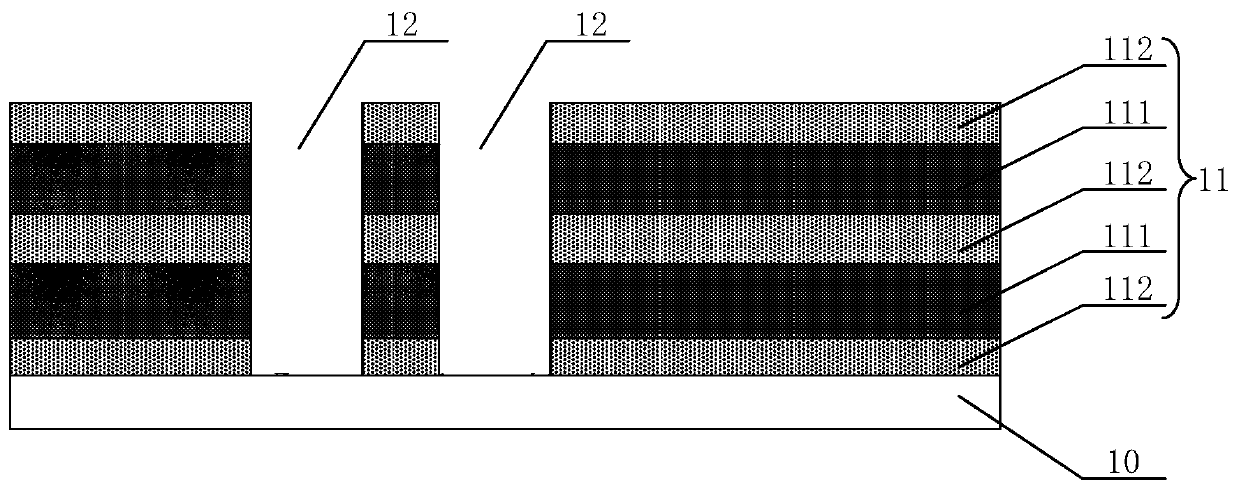
[0110]2) forming a channel via hole in the laminated structure, comprising the steps of: forming a vertical via hole in the laminated structure; removing part of the insulating dielectric layer by lateral etching based on the vertical via hole, forming a groove region between adjacent sacrificial layers and between the sacrificial layer and the semiconductor substrate;
[0111] 3) forming a functional sidewall on the surface of the sidewall of the channel through hole, and forming a channel layer on the surface of the functional sidewall and the bottom of the channel through hole; The portion between t...
Embodiment 2
[0189] see Figure 27 and Figure 28 , the present invention also provides a 3D NAND flash memory, the 3D NAND flash memory includes: a semiconductor substrate 10; a stacked structure 31, the stacked structure 31 is located on the semiconductor substrate 10, the stacked structure 10 includes Alternately stacked inter-gate dielectric layers 17 and gate layers 18, the inter-gate dielectric layer 17 includes alternately stacked first leakage suppression layers 171 and second leakage suppression layers 172; channel via holes 12, the channel The channel via hole 12 is located in the stacked structure 31; the channel via hole 12 includes a plurality of groove regions 122, and the groove region 122 is located between the adjacent gate layers 18 and the gate electrode Between the layer 18 and the semiconductor substrate 10; the functional sidewall 13, the functional sidewall 13 is located on the sidewall surface of the channel via hole 12, and the functional sidewall 13 is located ad...
PUM
 Abstract
Description
Claims
Application Information


