Display substrate and manufacturing method thereof, display panel and display device

A display substrate and manufacturing method technology, applied in the direction of electrical components, electric solid devices, circuits, etc., can solve the problems affecting the performance of OLED display substrates, and the inorganic film layer is prone to cracks, etc., to achieve the effect of improving long-term reliability and ensuring performance

Active Publication Date: 2019-07-30
BOE TECH GRP CO LTD
View PDF3 Cites 3 Cited by
  • Summary
  • Abstract
  • Description
  • Claims
  • Application Information

AI Technical Summary

Problems solved by technology

[0003] In the production of OLED display substrates, the OLED display substrate motherboard is cut by laser in the related art, but when cutting the OLED display substrate motherboard, the inorganic film layer is prone to cracks, and the cracks in the buffer zone m

Method used


Image

  • Display substrate and manufacturing method thereof, display panel and display device
  • Display substrate and manufacturing method thereof, display panel and display device
  • Display substrate and manufacturing method thereof, display panel and display device

Examples


Example Embodiment

[0060] In order to make the technical problems, technical solutions and advantages to be solved by the embodiments of the present invention clearer, the following will describe in detail with reference to the drawings and specific embodiments.

[0061] Embodiments of the present invention provide a display substrate and its manufacturing method, a display panel, and a display device, which can prevent cracks or cracks in the buffer inorganic film layer from being transmitted to the wiring area and even the inorganic film layer in the display area, and ensure the performance of the display substrate. , Improve the long-term reliability of the display substrate.

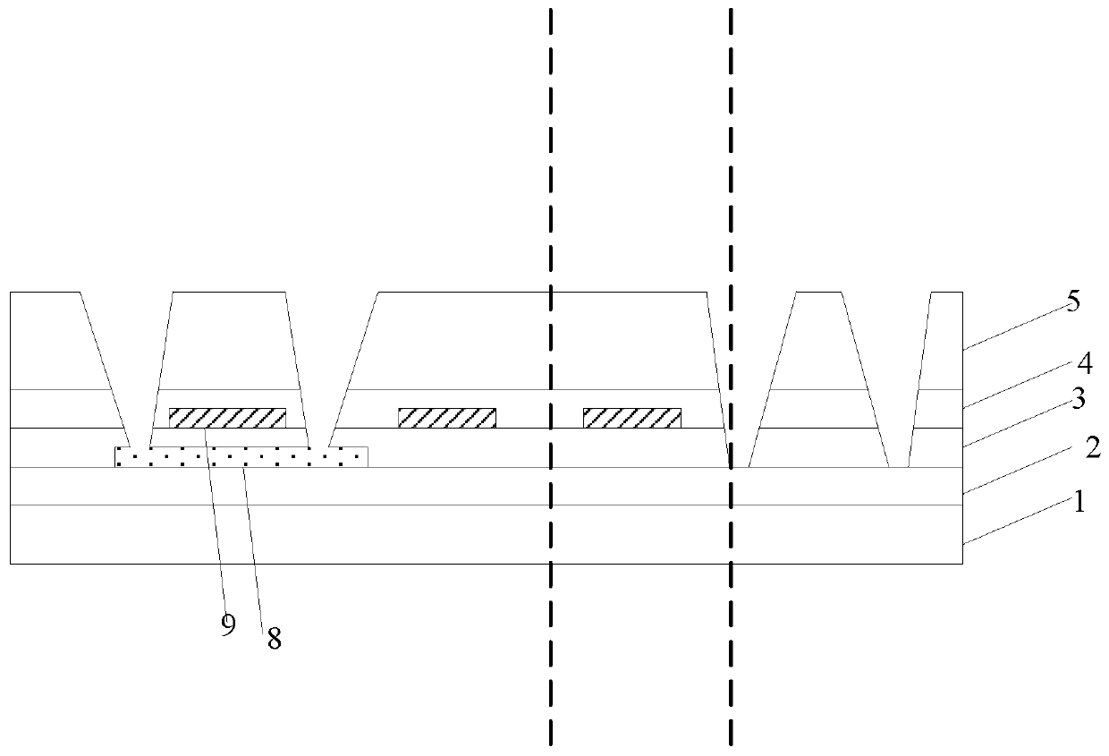
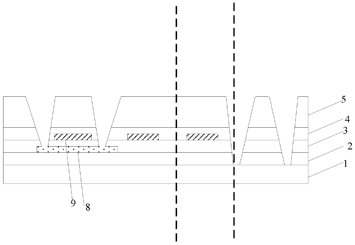
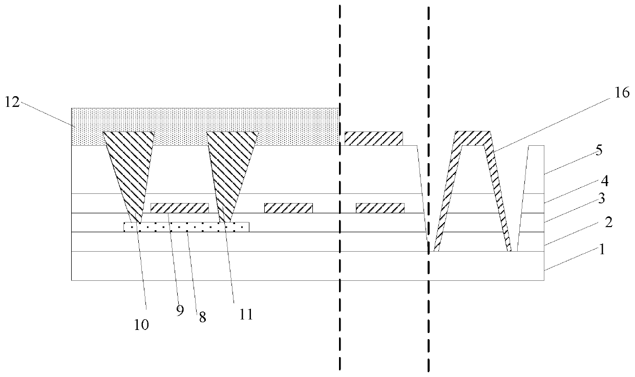
[0062] An embodiment of the present invention provides a display substrate motherboard, including a functional area and a buffer zone between the functional area and the boundary of the display substrate, the functional area includes a display area provided with an OLED display device and a buffer zone located between t...


PUM


Abstract

The invention provides a display substrate and a manufacturing method thereof, a display panel and a display device, and belongs to the technical field of display. The display substrate comprises a functional area and a buffer area located between the functional area and the boundary of the display substrate, wherein the functional area comprises a display area provided with an OLED display deviceand a routing area located around the display area, and the buffer area is provided with an inorganic film layer cut-off structure such that the inorganic film layer is discontinuous in the buffer area. The technical solution provided by the invention can prevent the crack of the inorganic film layer of the buffer area from being transmitted to the routing area even the inorganic film layer of the display area, ensure the performance of the display substrate and improve the long-term reliability of the display substrate.

Description

technical field [0001] The present invention relates to the field of display technology, in particular to a display substrate and a manufacturing method thereof, a display panel, and a display device. Background technique [0002] Organic electroluminescent display (OLED) has become the preferred technology for flexible display devices due to its advantages such as fast response speed, thin thickness, and high contrast ratio, especially its ability to be bendable and flexible. [0003] In the production of OLED display substrates, the OLED display substrate motherboard is cut by laser in the related art, but when cutting the OLED display substrate motherboard, the inorganic film layer is prone to cracks, and the cracks in the buffer zone may be transmitted to the display area The surrounding routing area and even the inorganic film layer in the display area cause water and oxygen in the air to enter the OLED display substrate along the cracks, affecting the performance of th...

Claims


Application Information

Patent Timeline
IPC IPC(8): H01L27/32
CPCH10K59/12H10K59/1201H10K59/124H10K50/8445H10K50/8426H10K50/844H10K50/846H10K50/8428H10K71/00
Inventor 徐传祥舒适姚琪袁广才
Owner BOE TECH GRP CO LTD
Why Eureka
Try Eureka