A diversion mechanism for semiconductor packaging equipment and its working method

A packaging equipment, semiconductor technology, applied in packaging, transportation and packaging, conveyor objects, etc., can solve the problems of time-consuming and labor-intensive, low degree of automation, inconvenient adjustment, etc., to achieve time-saving and labor-saving use, high degree of automation, and improved work efficiency Effect

Active Publication Date: 2020-12-01
合肥富芯元半导体有限公司
View PDF5 Cites 0 Cited by
  • Summary
  • Abstract
  • Description
  • Claims
  • Application Information

AI Technical Summary

Problems solved by technology

[0004] The purpose of the present invention is to solve the problem of the time-consuming and labor-intensive use of the existing semiconductor packaging equipment transfer mechanism, the low degree of automation of the work, and the low efficiency of semiconductor transfer and storage work, and the difficulty of semiconductor packaging and storage capacity. low, and the flexibility of the use of the transfer mechanism is poor, and the adjustment is inconvenient, and a semiconductor packaging equipment transfer mechanism and its working method are proposed

Method used


Image

  • A diversion mechanism for semiconductor packaging equipment and its working method
  • A diversion mechanism for semiconductor packaging equipment and its working method
  • A diversion mechanism for semiconductor packaging equipment and its working method

Examples


Embodiment Construction

[0044] The technical solutions of the present invention will be clearly and completely described below in conjunction with the embodiments. Apparently, the described embodiments are only some of the embodiments of the present invention, not all of them. Based on the embodiments of the present invention, all other embodiments obtained by persons of ordinary skill in the art without creative efforts fall within the protection scope of the present invention.

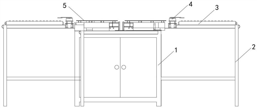
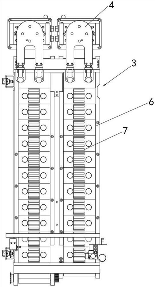
[0045] see Figure 1-11 As shown, a transporting mechanism for semiconductor packaging equipment includes a loading cabinet 1, two support platforms 2, a moving rack 3, a grasping platform 4 and a rotary seat 5, and the loading cabinet 1 is a hollow U-shaped structure, and Both ends of the loading cabinet 1 are provided with moving racks 3, above the moving rack 3 there is a grasping table 4, and above the loading cabinet 1 there are two swivel seats 5;

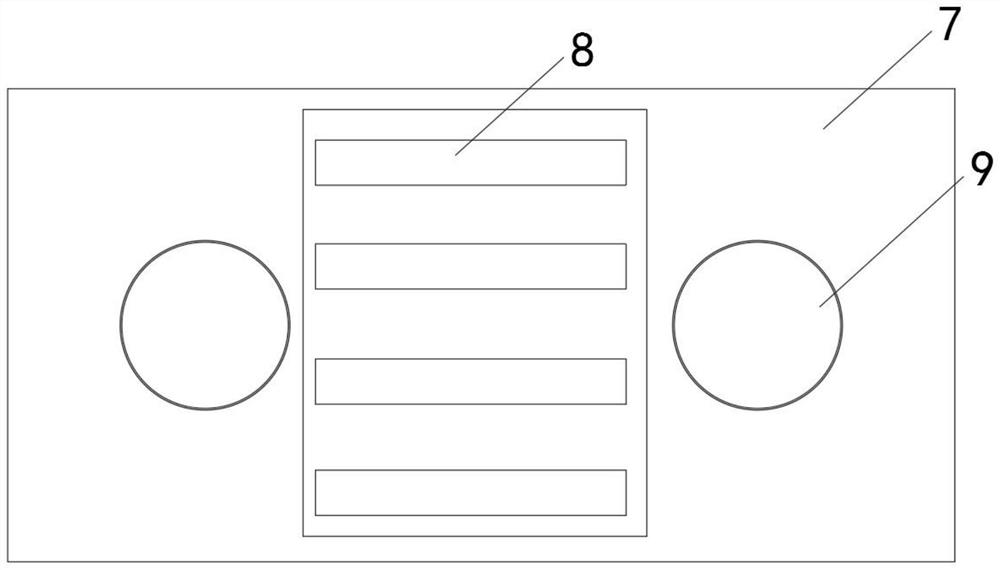
[0046] Transmission belts 6 are arranged on both sides of the two mo...


PUM


Abstract

The invention discloses a moving mechanism for semiconductor packaging equipment. The moving mechanism includes a carrying cabinet, two supporting platforms, moving frames, grabbing platforms and rotating seats. The carrying cabinet is of a hollow U-shaped structure. The moving frames are arranged on the two ends of the carrying cabinet. The grabbing platforms are arranged above the moving frames.The beneficial effects of the moving mechanism for semiconductor packaging equipment are that multiple storage blocks can be placed side by side on a transmission belt to accommodate semiconductors,multiple storage slots are arranged in parallel in each storage block at equal intervals, which can ensure that the mechanism can store a plurality of semiconductors at the same time for moving and loading and improves the working efficiency and the capacity of the mechanism, the storage blocks are clamped by clamping jaws I on the grabbing platforms, rotated and moved to the rotating seats, the rotating seats are driven by hydraulic pumps I to move down to store the semiconductors, the distance between the storage blocks and clamping and moving seats is detected by distance sensors, and the storage blocks are stored in the storage slots through the clamping and moving seats, which ensures that the mechanism is higher in work automation degree and more time-saving and more labor-saving inuse.

Description

technical field [0001] The invention relates to a diverting mechanism, in particular to a diverting mechanism for semiconductor packaging equipment and a working method thereof, belonging to the technical field of diverting mechanisms. Background technique [0002] When semiconductors are processed and produced, packaging equipment is required to package the semiconductors. After the packaging is completed, a diversion agency is required to transport, transfer and store the semiconductors, which is convenient for the semiconductors to be taken out later, packaged and used, and to ensure that after the semiconductors are processed, they will not Damaged by rubbing. [0003] There are still many deficiencies in the use of the existing diversion mechanism for semiconductor packaging equipment. The existing diversion mechanism for semiconductor packaging equipment is time-consuming and laborious in use, and the degree of automation of the work is low. The efficiency of the work...

Claims


Application Information

Patent Timeline
Patent Type & Authority Patents(China)
IPC IPC(8): B65B61/28B65G47/90
CPCB65B61/28B65G47/90
Inventor 王全沈春福周体志徐玉豹薛战吴海兵郑文彬
Owner 合肥富芯元半导体有限公司
Why Eureka
Try Eureka