Localized channel field effect transistor and preparation method thereof
A field effect transistor and localization technology, which is applied in the field of preparation of the field effect transistor to achieve the effects of reducing the minimum noise figure, improving the gain and linearity, and increasing the equivalent conductive cross-sectional area
- Summary
- Abstract
- Description
- Claims
- Application Information
AI Technical Summary
Problems solved by technology
Method used
Image

Examples
Embodiment Construction
[0019] The technical solution of the present invention will be further described in detail below in conjunction with the embodiments and the accompanying drawings.
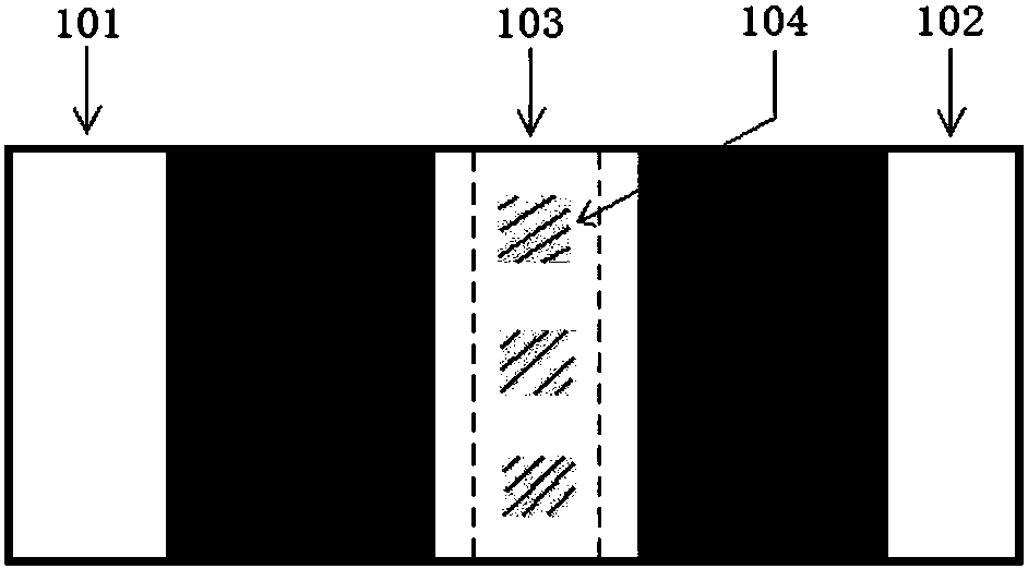
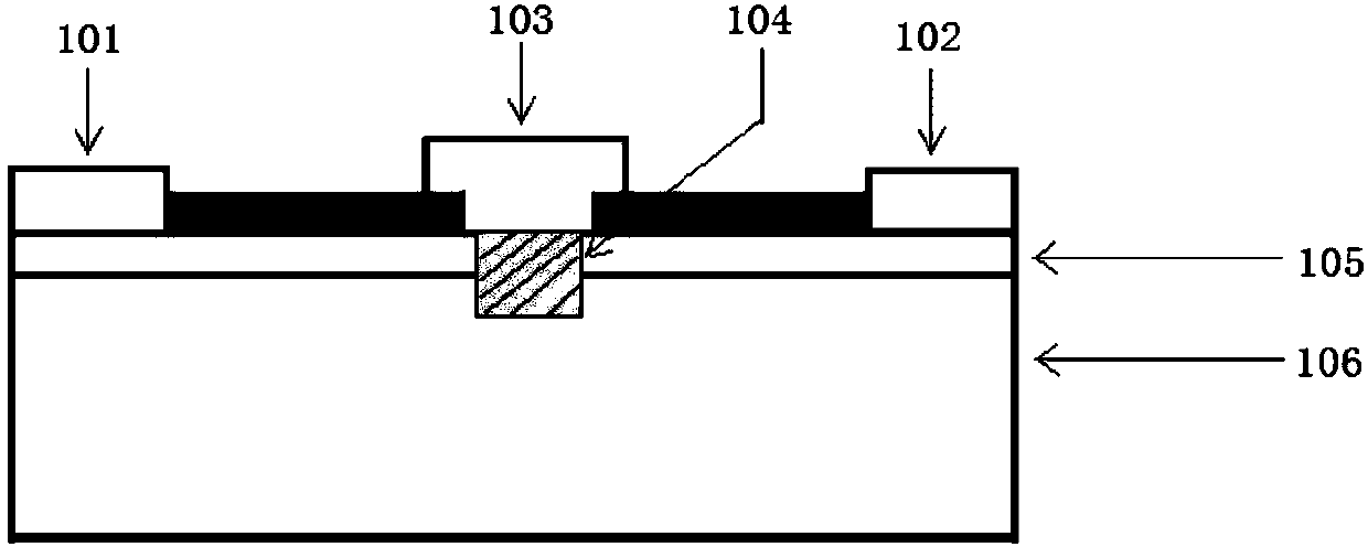
[0020] In this embodiment, the field effect transistor is a GaN high electron mobility transistor (HEMT), and the GaN HEMT structure of the localized channel structure is shown in Figure 1, wherein Figure 1 (a) is a top view of the device structure, and Figure 1 (b ) is a cross-sectional view of the device structure; 101 is a source, 102 is a drain, 103 is a gate, and 104 is a channel well, the channel well 104 is filled with a dielectric and covered by a gate metal, 105 is an AlGaN barrier layer, and 106 It is a GaN channel and a buffer layer, and the substrate layer is not shown in the figure; the localized trench field effect transistor structure proposed by the present invention is not limited to GaN HEMT, but can also be based on semiconductor materials such as Si and GaAs; the localized trench The channel st...
PUM
| Property | Measurement | Unit |
|---|---|---|
| Depth | aaaaa | aaaaa |
| Width | aaaaa | aaaaa |
Abstract
Description
Claims
Application Information