Threshold voltage drift detection method and threshold voltage drift detection device

A technology of threshold voltage drift and detection method, which is applied to instruments, static indicators, etc., and can solve problems such as inability to test the stability of array substrates

Active Publication Date: 2019-08-09
HEFEI XINSHENG OPTOELECTRONICS TECH CO LTD +1
View PDF7 Cites 6 Cited by
  • Summary
  • Abstract
  • Description
  • Claims
  • Application Information

AI Technical Summary

Problems solved by technology

[0004] The main purpose of the present invention is to provide a threshold voltage drift detection method and a threshold voltage drift detection device, which solve the problem that the array substrate (the arr

Method used


Image

  • Threshold voltage drift detection method and threshold voltage drift detection device
  • Threshold voltage drift detection method and threshold voltage drift detection device
  • Threshold voltage drift detection method and threshold voltage drift detection device

Examples


Embodiment approach

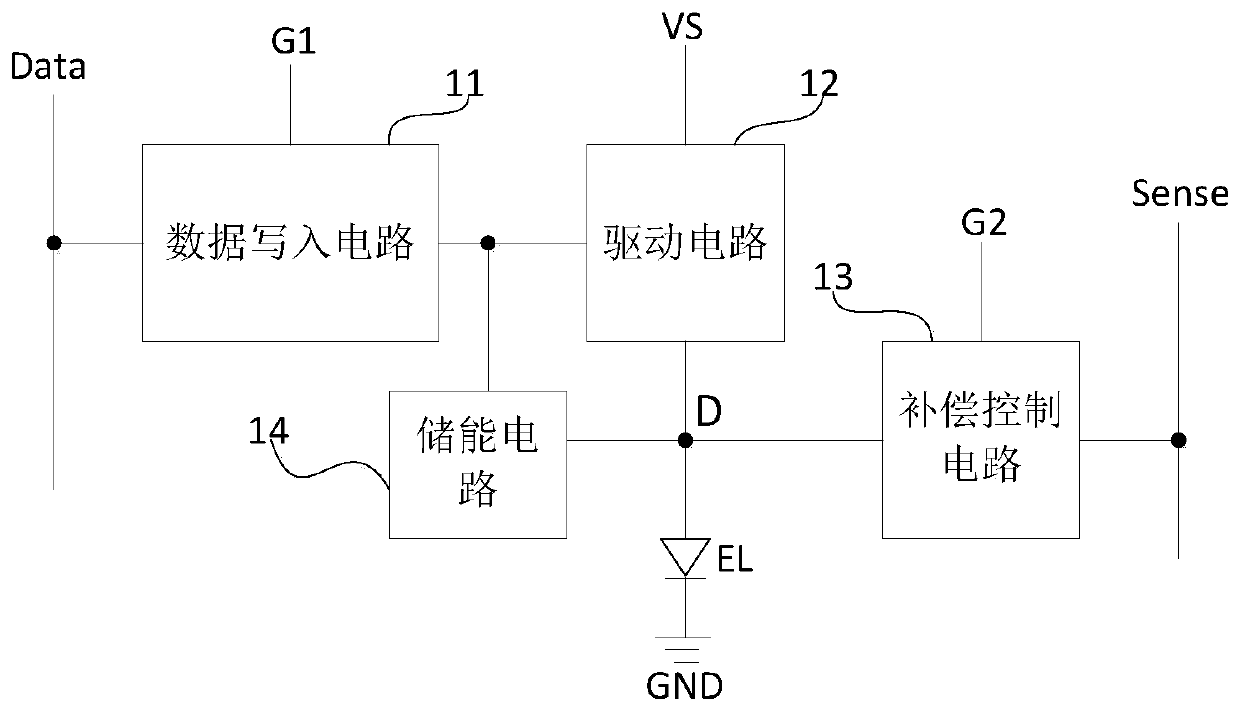
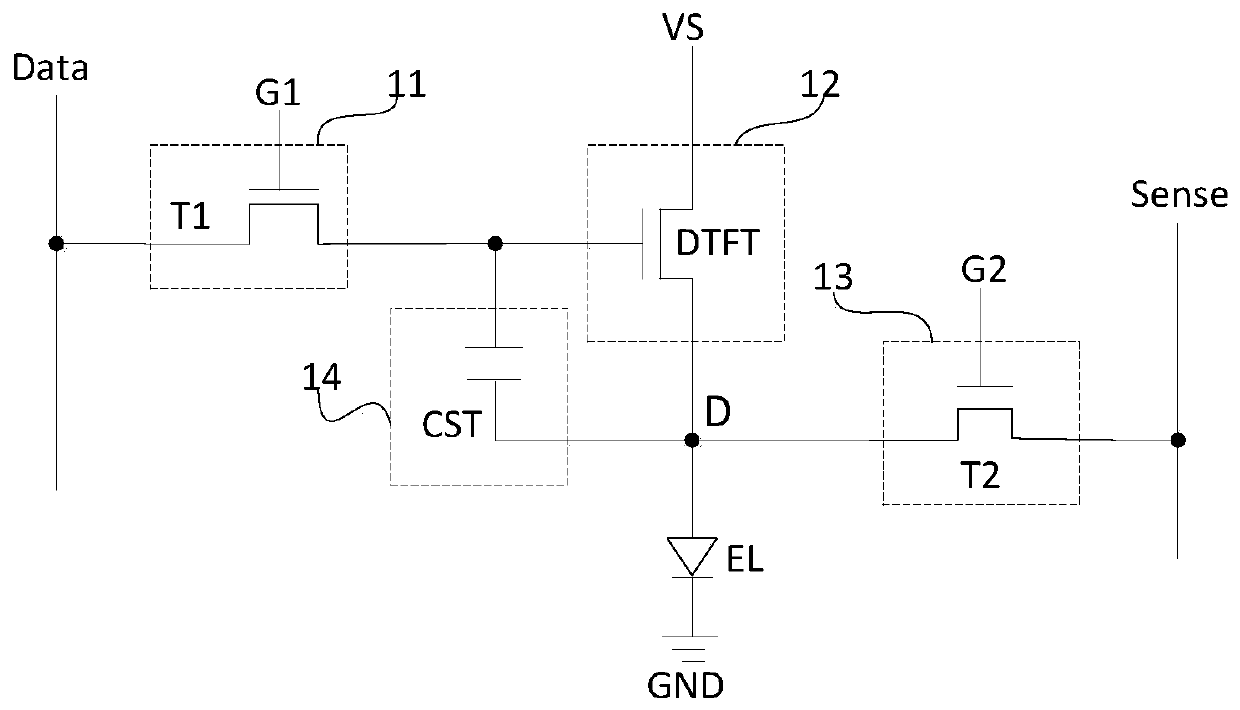
[0127] According to a specific implementation manner, the control pole of the driving transistor is the control terminal of the driving circuit, the first pole of the driving transistor is electrically connected to the power supply voltage line, and the second pole of the driving transistor is connected to the The detection node is electrically connected; the step of controlling a transistor included in the pixel driving circuit to be in a biased state during the setting phase may include:

[0128] In the set phase, a predetermined second data voltage is provided to the data line, and a third gate driving voltage signal is provided to the gate line, so that the data writing circuit controls to write the second data voltage writing into the control electrode of the driving transistor, and supplying a predetermined second power supply voltage to the power supply voltage line, so as to control the driving transistor to be in a bias state.

[0129] During specific implementation, ...


PUM


Abstract

The invention provides a threshold voltage drift detection method and a threshold voltage drift detection device. The threshold voltage drift detection method is applied to a pixel driving circuit, and the pixel driving circuit is electrically and separately connected with a control line, a voltage line and a detection node. The detection period comprises a setting stage and a detection stage, andthe threshold voltage drift detection method comprises the following steps of at the setting stage, controlling a transistor included in the pixel driving circuit to be in a bias state; and at the detection stage, providing a predetermined control voltage signal for the control line to provide a predetermined voltage signal for the voltage line, and judging the threshold voltage drift state of the transistor according to the potential of the detection node. According to the present invention, the bias temperature stress test can be directly carried out, and the threshold voltage drift state of the transistor included in the pixel driving circuit can be detected.

Description

technical field [0001] The invention relates to the field of display technology, in particular to a threshold voltage drift detection method and a threshold voltage drift detection device. Background technique [0002] In the prior art, when preparing a display substrate, a driving circuit layer (the driving circuit layer includes a pixel driving circuit) is first provided on the base substrate to form an array substrate, and then the pixel area BTS of the driving circuit layer needs to be performed. (BiasTemperature Stress, bias temperature stress) stability test, after the test is passed, the light emitting element is prepared on the driving circuit layer. [0003] In the prior art, the BTS stability test in the pixel area can only be performed through sample preparation or TEG (Test Element Group, test element group) near the pixel area. The BTS stability test method for sample preparation refers to: by slicing the array substrate, cutting the gate, source and drain of t...

Claims


Application Information

Patent Timeline
IPC IPC(8): G09G3/00
CPCG09G3/006G09G3/3225G09G2320/041G09G2320/0666G09G2320/0295G09G2330/12G09G2300/0426G09G2300/0809G09G2330/02
Inventor 李广耀王东方汪军王海涛郝朝威冯波刘融蔡伟罗标孙学超桂学海梁启斌万燕飞苏瑾
Owner HEFEI XINSHENG OPTOELECTRONICS TECH CO LTD
Why Eureka
Try Eureka